
SLIDE 1
1
C u r r e n t
- i
n d u c e d ma g n e t i z a t i
- n
d y n a mi c s i n n a n
- ma
g n e t
T e r u
- O
n
- I
n s t i t u t e f
- r
C h e mi c a l R e s e a r c h , K y
- t
- U
n i v e r s i t y
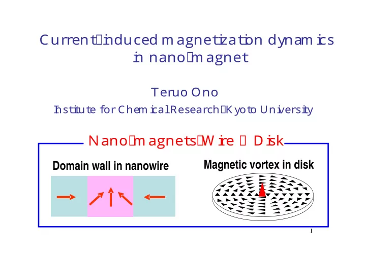
N a n
- ma