
SLIDE 1
1
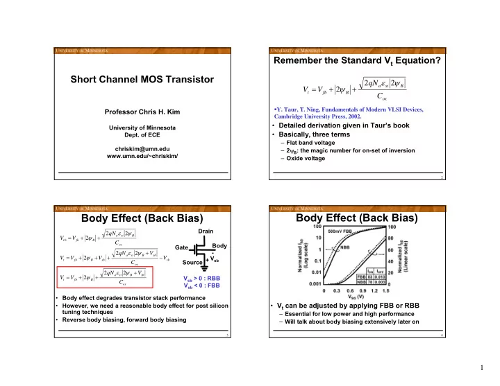
Short Channel MOS Transistor
Professor Chris H. Kim
University of Minnesota
- Dept. of ECE
chriskim@umn.edu www.umn.edu/~chriskim/
2
Remember the Standard Vt Equation?
- x
B si a B fb t
C qN V V ψ ε ψ 2 2 2 + + =
- Detailed derivation given in Taur’s book
- Basically, three terms
– Flat band voltage – 2ψB: the magic number for on-set of inversion – Oxide voltage
- Y. Taur, T. Ning, Fundamentals of Modern VLSI Devices,
Cambridge University Press, 2002.
3
Body Effect (Back Bias)
- x
sb B si a B fb t sb
- x
sb B si a sb B fb t
- x
B si a B fb t
C V qN V V V C V qN V V V C qN V V + + + = − + + + + = + + = ψ ε ψ ψ ε ψ ψ ε ψ 2 2 2 2 2 2 2 2 2
- Body effect degrades transistor stack performance
- However, we need a reasonable body effect for post silicon
tuning techniques
- Reverse body biasing, forward body biasing
Drain Gate Source Body +
- Vsb
Vsb > 0 : RBB Vsb < 0 : FBB
4
Body Effect (Back Bias)
- Vt can be adjusted by applying FBB or RBB