APPROPRIATE PROTECTIVE LAYER DESIGN TO PREVENT FILLER-INDUCED DAMAGE - - PDF document

appropriate protective layer design to prevent filler
SMART_READER_LITE
LIVE PREVIEW

APPROPRIATE PROTECTIVE LAYER DESIGN TO PREVENT FILLER-INDUCED DAMAGE - - PDF document

18 TH INTERNATIONAL CONFERENCE ON COMPOSITE MATERIALS APPROPRIATE PROTECTIVE LAYER DESIGN TO PREVENT FILLER-INDUCED DAMAGE IN PLASTICALLY- ENCAPSULATED MICROELECTRONIC PACKAGES S. Lee 1 * 1 Department of Materials Science & Engineering,


slide-1
SLIDE 1

18TH INTERNATIONAL CONFERENCE ON COMPOSITE MATERIALS

Abstract This work provides an appropriate protective layer design to prevent filler-induced damage in plastically-encapsulated LOC (lead-on-chip)

  • packages. It was found that the spherical silica

particles included in the plastic package body are trapped in the space between the top surface of the device and the bottom of the lead-frame. The particles could cause mechanical damage on a particular site of the integrated circuit pattern due to the thermal shrinkage of the plastic package body during a thermal cycling test. In particular, the filler- induced damage was observed only in protection layer-excluded regions such as a pad area. This work shows in detail how effectively the appropriate design of the protective layer such as polyimide contributes to the prevention of the filler-induced reliability degradation in plastic packages. 1.Introduction As a semiconductor device is encapsulated with the filler-embedded plastic resin, its active pattern could be subjected to large thermal displacement-induced stress due to thermal expansion difference between the silicon device and the package body during thermal-cycling. [1-4] It has been reported that an increase in the volume fraction of fillers or the proper selection of the average filler size is effective for lowering the coefficient of thermal expansion in the plastic package body. [4] On the other hand, in

  • rder to avoid the filler-induced damage in

plastically-encapsulated LOC packages, it has been also reported that the maximum filler size should be much smaller than the gap size between the chip and the lead-frame. [4] However, it is not so desirable to change the volume fraction or the maximum size of fillers because of various other criteria which are required in the micro-electronic package body. The present work shows how the filler-induced damage can be suppressed by polyimide design modification without changing the volume fraction or the maximum size of fillers in the package body.

  • Fig. 1 Schematic drawing of LOC (lead-on-chip)

structure.

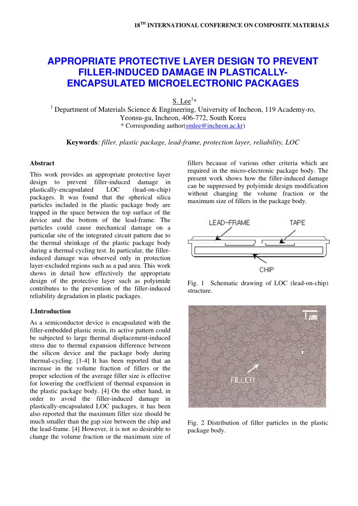
  • Fig. 2 Distribution of filler particles in the plastic

package body.

APPROPRIATE PROTECTIVE LAYER DESIGN TO PREVENT FILLER-INDUCED DAMAGE IN PLASTICALLY- ENCAPSULATED MICROELECTRONIC PACKAGES

  • S. Lee1*

1 Department of Materials Science & Engineering, University of Incheon, 119 Academy-ro,

Yeonsu-gu, Incheon, 406-772, South Korea

* Corresponding author(smlee@incheon.ac.kr)

Keywords: filler, plastic package, lead-frame, protection layer, reliability, LOC

slide-2
SLIDE 2
  • Fig. 3. Thermal-cycling profile.

2 Experiments All of the test devices were prepared through conventional VLSI circuit fabrication. Al alloys containing 1% Si were sputter-deposited to a thickness of 0.8 ㎛ on thermally grown oxide (SiO2) and then passivated by the PECVD (plasma- enhanced-chemical vapor deposition) technique. [2] Passivation materials consist of Si3N4 of 4000Å in

  • thickness. All dies were assembled in plastically-

encapsulated packages utilizing an LOC (lead-on- chip) die attach technique, as shown in Fig. 1. [2] Spherical silica particles are used as inorganic filler to lower the coefficient of thermal expansion in the present microelectronic molding compound, possibly leading to lower thermal shrinkage force on the chip surface. The level of fillers in the present package body is approximately 80% volume and the distribution of the filler size is in the range of 1 to 100 ㎛, as shown in Fig. 2. The chip size was 5.5mm x 11mm x 0.2mm and its package dimension was 6.5mm x 13mm x 0.5mm. In this LOC structure, the Fe-Ni lead-frame of 150um in thickness is mounted

  • n the top surface of each device using a double-

sided adhesive tape whose thickness is 60um. In

  • rder to investigate filler-induced failure due to the

thermal shrinkage of a plastic package body, all reliability tests were confined to thermal-cycling. Test specimens underwent thermal displacement- induced fatigue at a temperature range of -65oC to 150 oC within a 30 minute time period, as shown in

  • Fig. 4. Scanning electron micrograph showing a

filler-induced damage on the activepattern after thermal-cycling.

  • Fig. 3. Predetermined time to validate reliability was

1000 cycles for temperature-cycling. Predetermined time to validate reliability was 1000 cycles for temperature-cycling. For each set of experiments, nominally identical specimens were placed in the thermal cycle chamber, then individual specimens were functionally tested after predetermined periods. Once any functional failure was found, the corresponding specimens were decapsulated and examined under an optical microscope (OM) and scanning electron microscope (SEM) to identify the filler-induced damage.

  • 3. Results

3.1. Filler-Induced Damage It was observed in the present research that when a package body includes large fillers that is similar to the inter-distance between the silicon chip and the lead-frame, the device pattern becomes more susceptible for filler-induced damage as shown in

  • Fig. 4. Therefore, to reduce the maximum size of the

fillers included in the plastic package body was very important for the prevention of the filler-induced damage in the present package structure. In addition, the metallurgical examination indicates that the filler-induced damage took place on a particular region of the passivation layer (i.e. Si3N4) where the protection layer (i.e. ductile polyimide) is

  • 80
  • 60
  • 40
  • 20

20 40 60 80 100 120 140 160 10 20 30 40 50 60

Time (minutes) Temperature (℃)

slide-3
SLIDE 3

3 PAPER TITLE

(a) (b)

  • Fig. 5 Scanning electron micrograph showing the

different pattern design of the polyimide layer; a) conventional design, and b) advanced design. locally absent for electric connection. The passivation layer adopted in the present device has a thickness of approximately 4000Å, which is much smaller than the trapped filler between the device and the lead-frame. Thus, if such a thin and brittle passivation layer beneath the trapped filler fails to accommodate the filler-induced compressive force, it would be broken. So, in order to avoid the filler- induced damage, we need an appropriate design of the protection layer that is ductile enough to carry

  • ut a role of buffering against the filler-induced

compressive force. It was tested in this work how manipulating the design of the protection layer affects the filler-induced reliability of LOC packages. The present protection layer is polyimide with a thickness of 10 ㎛ , which is ductile enough to accommodate filler-causing compressive force. 3.2. Appropriate Polyimide Design Two different patterns of the protective layer around pad regions were shown in Fig. 5. In the conventional design of the protective layer, a broad area of the polyimide layer was eliminated to allow a large opening region to include several pads through the chemical etching process, as shown in Fig. 5a. On the other hand, in the advanced design of the protection layer, a smaller part of the polyimide layer was removed to provide a minimum opening region for each pad. The device surface with the advanced polyimide design is shown in Fig. 5b where the brittle passivation layer is overcoated with ductile polyimide except the pad area for the fuse connection at the center area of the device. Consequently, the conventional design results in larger opening area of polyimide around pad regions, while the advanced design allows more effective coverage of polyimide around each pad, as shown in

  • Fig. 5.

The number of filler-induced failures in two different types of devices (the conventional design and the advanced design of polyimide) was estimated as a function of the maximum size of the

  • fillers. The experimental data are shown in Fig. 6.

The result indicates that as the size of the largest filler included in a given package body is smaller than half of the inter-distance between the device and the lead-frame, no filler-induced failure was

  • bserved regardless of the design of the protective
  • layer. On the other hand, the specimens including

the fillers with a size that is similar to the inter- distance between the device and its overlying lead- frame have different failure aspects, depending on the design of the protective layer. That is, the devices with the advanced polyimide design revealed much fewer failures as compared to the devices with the conventional design even though it did not work perfectly. Consequently, it is clear from the present research that the limited exclusion

  • f polyimide at the pad region can suppress the

susceptibility of the device pattern to filler-induced

  • damage. As was mentioned before, it is important to

reduce the potential of the filler-induced damage through the change of the polyimide layout since it might not be desirable to manipulate the volume fraction or the maximum size of fillers because of their various other criteria.

slide-4
SLIDE 4
  • Fig. 6. A graph showing the number of filler-

induced failures as a function of the size of fillers embedded in the package body representing a large number of failures at the size of approximately 60 ㎛. (a) (b)

  • Fig. 7. Schematics showing how filler-induced

failure is influenced by the protection layer design; a) conventional design, and b) advanced design.

  • 4. Discussion

The reason why there still exist a few failures even in the devices with the advanced design (as shown in

  • Fig. 6) is explained in the following. Prior to thermal

cycling, there should be the filler trapped between the hard silicon device and its overlying lead-frame. Then, the trapped filler would be pressed by the lead-frame embedded in the package body during the thermal displacement-induced warpage of the plastic package body during a thermal cycling test. If the trapped filler lies on the brittle passivation layer

  • f the device pattern, it could develop the

compressive force from the lead-frame into a large stress because of its hard underlying layer. Consequently, a large compressive stress could be applied at the specific region of the device pattern due to the trapped filler, as illustrated in Fig. 7. In the conventional design, the device pattern might be more likely to be exposed to the filler-induced damage due to the broader opening region of polyimide, as shown in Fig. 7a. On the other hand, in the advanced design, the devices might have fewer probabilities to be exposed to the filler- induced damage due to more effective coverage of polyimide, as shown in Fig. 7b. That explains why the devices with the advanced polyimide design cause much less filler-induced failures (in particular, when the fillers have a damage-causing size). Therefore, we can predict that if the full coverage of the protection layer over the entire passivation layer is allowed, the filler-induced damage would be completely prevented. In fact, the imperfect coverage of polyimide is due to a technical limitation in chemical etching for the opening of

  • polyimide. This technical issue is out of the present

scope but such a limitation might be overcome by the adoption of other advanced opening techniques. Consequently, in order to avoid the filler-induced reliability degradation in plastically-encapsulated LOC packages, the exclusion of the polyimide layer for electric connection should be minimized.

  • 5. Conclusions

This work presented that the spherical silica particles included in the plastic package body might directly attack a very thin and brittle layer such as Si3N4 of the device pattern during thermal-cycling. So, it was investigated whether manipulating the design of the protection layer, which is ductile polymer and has a thickness of 10 ㎛, can influence the filler-causing

  • failure. The experimental results suggested that the

appropriate design of polyimide is very effective for reducing the occurrence of filler-induced failure

2 4 6 8 10 12 14 20 40 60 80 100

Number of failure Maximum filler size (um)

Less cover Full cover

slide-5
SLIDE 5

5 PAPER TITLE

even though it was not enough for the complete prevention of filler-induced damage. That is, in

  • rder to avoid filler-induced damage in plastic LOC

packages, the exclusion of the protection layer for electric connection should be minimized. The minimum removal of the polyimide layer might allow a greater reliability margin for the selection of the packaging materials in the LOC package structure. References

[1] L.T. Manzione “Plastic Packaging of Micro-

electronic Devices” Van Nostrand Reinhold, New York, 2000.

[2] S. Lee "Thermal stress-induced failure in

memory device assembled using lead-on-chip die attach technique" Jpn. J. Appl. Phys., Vol. 41, 6A, pp. 3860-3865, 2002.

[3] R. Tummala, "Microelectronics packaging hand-

book", Van Nostrand Reinhold, New York, 2004.

[4] S. Lee “Filler-induced failure mechanism in

plastic-encapsulated microelectronic packages”. Metals and Materials International, Vol. 12, No. 6, pp. 513-516, 2006. .