analog electronic circuits prof mor m peretz
play

Analog Electronic Circuits Prof. Mor M. Peretz The Center for Power - PDF document

4/15/2018 [1] PE Prof. Mor M. Peretz Analog Electronic Circuits 361-1-3671 M I T HE C ENTER FOR P OWER E LECTRONICS AND M IXED -S IGNAL IC, B EN -G URION U NIVERSITY C BGU Analog Electronic Circuits Prof. Mor M. Peretz The Center for


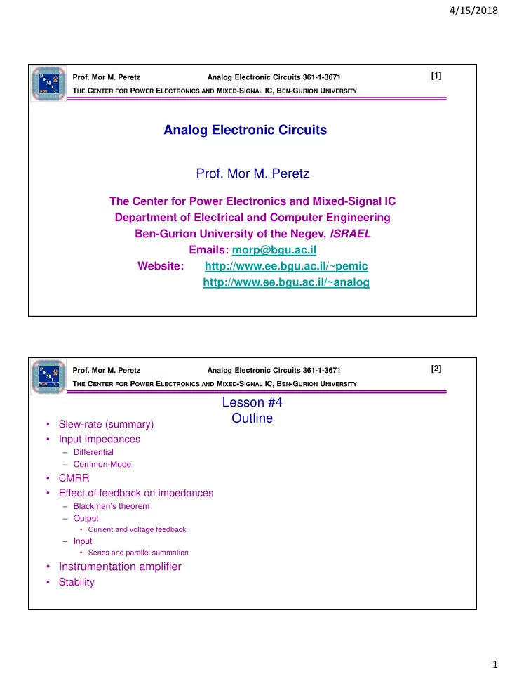
  1. 4/15/2018 [1] PE Prof. Mor M. Peretz Analog Electronic Circuits 361-1-3671 M I T HE C ENTER FOR P OWER E LECTRONICS AND M IXED -S IGNAL IC, B EN -G URION U NIVERSITY C BGU Analog Electronic Circuits Prof. Mor M. Peretz The Center for Power Electronics and Mixed-Signal IC Department of Electrical and Computer Engineering Ben-Gurion University of the Negev, ISRAEL Emails: morp@bgu.ac.il Website: http://www.ee.bgu.ac.il/~pemic http://www.ee.bgu.ac.il/~analog [2] PE Prof. Mor M. Peretz Analog Electronic Circuits 361-1-3671 M I T HE C ENTER FOR P OWER E LECTRONICS AND M IXED -S IGNAL IC, B EN -G URION U NIVERSITY C BGU Lesson #4 Outline • Slew-rate (summary) • Input Impedances – Differential – Common-Mode • CMRR • Effect of feedback on impedances – Blackman’s theorem – Output • Current and voltage feedback – Input • Series and parallel summation • Instrumentation amplifier • Stability 1

  2. 4/15/2018 [3] PE Prof. Mor M. Peretz Analog Electronic Circuits 361-1-3671 M I T HE C ENTER FOR P OWER E LECTRONICS AND M IXED -S IGNAL IC, B EN -G URION U NIVERSITY C BGU Transient response Slew-Rate 𝑇𝑆 = 𝑗 𝐶 𝑇𝑆 𝐷 𝑓𝑟 𝑊 𝑛_𝑝𝑣𝑢 = 𝑛𝑗𝑜 , 𝑊 Sine wave 𝑡𝑏𝑢 2𝜌𝑔 𝑛 V out V m_out V sat V in V out_SR 8V 800mV 80mV f m [Hz] 1M 100K 1K 10K [4] PE Prof. Mor M. Peretz Analog Electronic Circuits 361-1-3671 M I T HE C ENTER FOR P OWER E LECTRONICS AND M IXED -S IGNAL IC, B EN -G URION U NIVERSITY C BGU Input Impedances V1 - Vd/2 V OUT + R d 𝑑𝑛 = 𝑊 1 + 𝑊 + 2 𝑊 2 𝑊 𝑒 = 𝑊 1 − 𝑊 R cm 2 R cm Vcm + + Vd/2 V2 2

  3. 4/15/2018 [5] PE Prof. Mor M. Peretz Analog Electronic Circuits 361-1-3671 M I T HE C ENTER FOR P OWER E LECTRONICS AND M IXED -S IGNAL IC, B EN -G URION U NIVERSITY C BGU Input Impedances Differential VCC ℎ 𝑗𝑓 = 𝑊 𝑈 ℎ 𝑔𝑓 + 1 𝐽 𝑓 𝑆 𝑒 = 2ℎ 𝑗𝑓 = 2 𝑊 𝑈 𝐽 𝑓 ℎ 𝑔𝑓 + 1 OUT IN- IN+ Q 1 Q 2 R in VEE [6] PE Prof. Mor M. Peretz Analog Electronic Circuits 361-1-3671 M I T HE C ENTER FOR P OWER E LECTRONICS AND M IXED -S IGNAL IC, B EN -G URION U NIVERSITY C BGU Input Impedances Common-mode VCC 𝑆 𝑓 = 1 ℎ 𝑝𝑓 OUT 𝑆 𝑑𝑛 = 2𝑆 𝑓 ℎ 𝑔𝑓 + 1 IN- IN+ Q 1 Q 2 V EE R in VEE 3

  4. 4/15/2018 [7] PE Prof. Mor M. Peretz Analog Electronic Circuits 361-1-3671 M I T HE C ENTER FOR P OWER E LECTRONICS AND M IXED -S IGNAL IC, B EN -G URION U NIVERSITY C BGU Common-Mode Rejection Ratio (CMRR) 𝐷𝑁𝑆𝑆 ≡ 𝐵 𝑒 = 𝐵 𝑒 𝐵 2 𝐵 3 𝑊 𝑑𝑛 = 0 R 1 𝐵 𝑑𝑛 𝐵 𝑑𝑛 𝐵 2 𝐵 3 R 2 V 2 V in - V OUT V 1 + 𝑑𝑛 = 𝑊 1 + 𝑊 2 𝑊 2 𝑊 𝑒 = 𝑊 1 − 𝑊 2 V 1 + V OUT V in V 2 - 𝑊 1 + 𝑊 2 𝑊 𝑝𝑣𝑢_𝑑𝑛 = 𝐵 𝑑𝑛 𝑊 𝑑𝑛 = 𝐵 𝑑𝑛 R 1 2 R 2 𝑊 𝑑𝑛 = 𝑊 𝑗𝑜 [8] PE Prof. Mor M. Peretz Analog Electronic Circuits 361-1-3671 M I T HE C ENTER FOR P OWER E LECTRONICS AND M IXED -S IGNAL IC, B EN -G URION U NIVERSITY C BGU Common-Mode Rejection Ratio (CMRR) 𝑊 𝑑𝑛 = 0 R 1 𝑊 𝑝𝑣𝑢 = 𝐵 𝑑𝑛 𝑊 𝑑𝑛 + 𝐵 𝑒 𝑊 𝑒 R 2 V 2 V in - V OUT 𝑊 𝑊 Reflected to input 𝑝𝑣𝑢 𝑑𝑛 𝐷𝑁𝑆𝑆 + 𝑊 𝐵 𝑒 = V 1 𝑒 + (as done to ALL non-idealities) V 1 + V OUT V in V 2 - R 1 R 2 𝑊 𝑑𝑛 = 𝑊 𝑗𝑜 4

  5. 4/15/2018 [9] PE Prof. Mor M. Peretz Analog Electronic Circuits 361-1-3671 M I T HE C ENTER FOR P OWER E LECTRONICS AND M IXED -S IGNAL IC, B EN -G URION U NIVERSITY C BGU Blackman’s Theorem 1+𝛾𝐵 𝑇𝐷 𝑎 𝐺 = 𝑎 𝑂𝐺 1+𝛾𝐵 𝑃𝐷 Load Load V’ in V’ in V in V e V in V e + - A OL + - A OL G G V out I out V f V f β β Voltage feedback Current feedback 𝑎 𝑂𝐺 𝑎 𝐺 = 𝑎 𝐺 = 𝑎 𝑂𝐺 1 + 𝛾𝐵 1+𝛾𝐵 [10] PE Prof. Mor M. Peretz Analog Electronic Circuits 361-1-3671 M I T HE C ENTER FOR P OWER E LECTRONICS AND M IXED -S IGNAL IC, B EN -G URION U NIVERSITY C BGU Effect of feedback Output impedance Voltage feedback Current feedback V 1 + I out V OUT V in V ref + V 2 - - R 1 R 2 R 1+𝛾𝐵 𝑇𝐷 1+𝛾𝐵 𝑇𝐷 𝑎 𝑝𝑣𝑢_𝐺 = 𝑆 0 𝑎 𝑝𝑣𝑢_𝐺 = 𝑆 0 1+𝛾𝐵 𝑃𝐷 1+𝛾𝐵 𝑃𝐷 5

  6. 4/15/2018 [11] PE Prof. Mor M. Peretz Analog Electronic Circuits 361-1-3671 M I T HE C ENTER FOR P OWER E LECTRONICS AND M IXED -S IGNAL IC, B EN -G URION U NIVERSITY C BGU Effect of feedback Example [ dB ] V 1 + A OL V OUT V in 100 V 2 - R 1 R 0 R 2 40 1/ β 20 R1=10k R2=1k f [ Hz ] R0=100 Z out_F -40 [12] PE Prof. Mor M. Peretz Analog Electronic Circuits 361-1-3671 M I T HE C ENTER FOR P OWER E LECTRONICS AND M IXED -S IGNAL IC, B EN -G URION U NIVERSITY C BGU Linear regulator Low-Drop Out (LDO) Z out_F + Z Load Vout 6

  7. 4/15/2018 [13] PE Prof. Mor M. Peretz Analog Electronic Circuits 361-1-3671 M I T HE C ENTER FOR P OWER E LECTRONICS AND M IXED -S IGNAL IC, B EN -G URION U NIVERSITY C BGU Effect of feedback Input impedance + β R 1 V in A V e V OUT - R 2 V in - R 1 V OUT V e + R 2 V f Parallel (current) summation Series (voltage) summation 𝑎 𝑂𝐺 𝑎 𝑗𝑜_𝐺 = 1+𝛾𝐵 𝑎 𝑗𝑜_𝐺 = 𝑎 𝑂𝐺 1 + 𝛾𝐵 [14] PE Prof. Mor M. Peretz Analog Electronic Circuits 361-1-3671 M I T HE C ENTER FOR P OWER E LECTRONICS AND M IXED -S IGNAL IC, B EN -G URION U NIVERSITY C BGU Input Impedances R 1 R 1 R 2 R 2 V 2 V 1 V in - - V OUT V OUT V Ɛ R 3 V 2 V 1 + 𝑆 1 +𝑠 0 + 𝑆 𝑗𝑜 = 𝑆 2 + 1+𝛾𝐵 ≈ 𝑆 2 R 4 𝑆 𝑗𝑜_1 = 𝑆 2 V 1 + 𝑆 𝑗𝑜_2 = 𝑆 3 + 𝑆 4 V OUT V in 𝑆 𝑗𝑜_1,2 = 𝑆 2 + 𝑆 3 V 2 - R 1 𝑆 𝑗𝑜 = 𝑆 𝑒 1 + 𝛾𝐵 R 2 7

  8. 4/15/2018 [15] PE Prof. Mor M. Peretz Analog Electronic Circuits 361-1-3671 M I T HE C ENTER FOR P OWER E LECTRONICS AND M IXED -S IGNAL IC, B EN -G URION U NIVERSITY C BGU Difference Amplifier R 1 R 2 V 1 - R 1 V OUT V Ɛ R 3 - V 2 R 2 + - V OUT V 1 + V Ɛ R 4 R 3 + V 2 + R 4 𝑆 1 𝑊 𝑝𝑣𝑢_1 = −𝑊 1 𝑆 2 - 𝑆 4 1 + 𝑆 1 𝑊 𝑝𝑣𝑢_2 = 𝑊 2 𝑆 3 + 𝑆 4 𝑆 2 𝑆 2 𝑆 3 𝑆 1 = 𝑆 4 𝑝𝑣𝑢 = 𝑆 1 𝑊 𝑊 2 − 𝑊 1 𝑆 2 [16] PE Prof. Mor M. Peretz Analog Electronic Circuits 361-1-3671 M I T HE C ENTER FOR P OWER E LECTRONICS AND M IXED -S IGNAL IC, B EN -G URION U NIVERSITY C BGU Instrumentation Amplifier V 1 𝑝𝑣𝑢 = 𝑆 1 + 𝑊 𝑊 𝑏𝑛𝑞_𝑐 − 𝑊 𝑏𝑛𝑞_𝑏 V amp_a 𝑆 2 - 𝐽 𝑦 = 𝑊 1 − 𝑊 2 R a 𝑆 𝑦 R 1 R 2 - 𝑊 𝑏𝑛𝑞_𝑐 − 𝑊 𝑏𝑛𝑞_𝑏 = 𝐽 𝑦 𝑆 𝑦 + 𝑆 𝑏 + 𝑆 𝑐 V OUT R x V Ɛ R 3 + 𝑝𝑣𝑢 = 𝑆 1 1 + 𝑆 𝑏 + 𝑆 𝑐 𝑊 𝑊 2 − 𝑊 R 4 1 𝑆 2 𝑆 𝑦 R b - V amp_b + V 2 8

  9. 4/15/2018 [17] PE Prof. Mor M. Peretz Analog Electronic Circuits 361-1-3671 M I T HE C ENTER FOR P OWER E LECTRONICS AND M IXED -S IGNAL IC, B EN -G URION U NIVERSITY C BGU Loop-Gain Nyquist Criterion 𝐵 𝑃𝑀 𝑡 𝐵 𝐷𝑀 = 𝐻 𝑡 1 + 𝛾𝐵 𝑃𝑀 𝑡 • The system is unstable if the characteristic equation {1+ β A OL (s)} has roots in the right half of the complex plane • Nyquist criterion is a test for location of {1+ β A OL (s)} roots • Nyquist criterion can be viewed on the frequency domain (Bode) [18] PE Prof. Mor M. Peretz Analog Electronic Circuits 361-1-3671 M I T HE C ENTER FOR P OWER E LECTRONICS AND M IXED -S IGNAL IC, B EN -G URION U NIVERSITY C BGU Loop-gain on the frequency domain |LG| [dB]      X’ in f A f X out X in X e + - A OL G X f f β   +180 f 0 In negative feedback o    o systems 180 ( 180 ) At f  0 9

  10. 4/15/2018 [19] PE Prof. Mor M. Peretz Analog Electronic Circuits 361-1-3671 M I T HE C ENTER FOR P OWER E LECTRONICS AND M IXED -S IGNAL IC, B EN -G URION U NIVERSITY C BGU Bode plot Phase margin [dB]  A  A  1 f   f 0          o o ( 180 ) 180 m     m | A | 1 | A | 1 -180 [20] PE Prof. Mor M. Peretz Analog Electronic Circuits 361-1-3671 M I T HE C ENTER FOR P OWER E LECTRONICS AND M IXED -S IGNAL IC, B EN -G URION U NIVERSITY C BGU Graphical representation of β A OL conventional method A [ dB ] AB [ dB ] A AB f [ Hz ] B [ dB ] f [ Hz ] B f f f 1 2 3 f [ Hz ] f f f 1 2 3  Tedious – need to re-plot BA  Analysis (not design) oriented  Requires iterations 10

  11. 4/15/2018 [21] PE Prof. Mor M. Peretz Analog Electronic Circuits 361-1-3671 M I T HE C ENTER FOR P OWER E LECTRONICS AND M IXED -S IGNAL IC, B EN -G URION U NIVERSITY C BGU Graphical Representation of β A OL 1   20log A 20log 20log(BA) B A [ dB ] A 1     20logA 20log B A 1 B BA   1 LG ( f ) BA 1 B BA BA  1 BA  1 f o [ Hz ] [22] PE Prof. Mor M. Peretz Analog Electronic Circuits 361-1-3671 M I T HE C ENTER FOR P OWER E LECTRONICS AND M IXED -S IGNAL IC, B EN -G URION U NIVERSITY C BGU Possible compensations Rate of Closure (ROC)   o 90   o m 45 m   o 90 m   o 45 m db 0   o 90 dec 1 m  20 db dec   o  45 m A s db u |A|  db 40 s  dec f db 20 u db 0 dec dec s   db db 20 60 dec dec f s  db 40 1 dec B db 11

Download Presentation
Download Policy: The content available on the website is offered to you 'AS IS' for your personal information and use only. It cannot be commercialized, licensed, or distributed on other websites without prior consent from the author. To download a presentation, simply click this link. If you encounter any difficulties during the download process, it's possible that the publisher has removed the file from their server.

Recommend


More recommend