
SLIDE 1
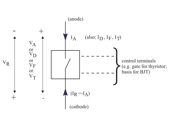
IA (anode) (cathode) (IR =-IA) control terminals (e.g. gate for thyristor; basis for BJT) (also: ID , IF , IT) VA
- r
VD
- r
VF
- r
VT
+
- +
- VR
- + (also: ID , IF , IT) IA VA or VD or control terminals VR - - PowerPoint PPT Presentation
(anode) - + (also: ID , IF , IT) IA VA or VD or control terminals VR VF (e.g. gate for thyristor; or basis for BJT) VT (IR =-IA) + - (cathode) IA conducting I F range forward current (1V) (100A) forward voltage drop A A
(a) p n p n A K (b) G A K G +
(VD ) (VT) VA reverse leakage current IA VBR reverse blocking range reverse (or avalanche) breakdown IG3>IG2>IG1>IG=0 conducting area forward breakover voltage forward blocking range IH IA (ID) (I T) (c)
VGT VGD IGD a b d c VG IG a limit the conducting range b of the G-K diode c maximal value for the control power (PGmax) d recommended load line
VGT , IGT : gate voltage and gate current above which every thyristor should start to conduct VGD , IGD : gate voltage and gate current below which no thyristor should start to conduct IGT
K
n + n + n + n + p + p + p + p + n
IC VCE saturation parameter IB (c) B E C IB IC + _ VCE C B E (a) (b) npn E B C (e) VCE iC1 <iC2<iC3 usable range (d) IB N P N Darlington
IDS Drain VDS VGS Source Gate + _ + _ (b) (a)
Al Gate Source SiO2
N+-Polysilicium
N+ N+ Drain P N _
2 1 3 4 5 6 7 8 9 10 2 4 6 8 10 20 10 30 40 50 60 70 80 90 100 200 400 600 800 1000 IDS IDS VDS VDS
V = 15V
GS
V = 10V
GS
5V 4V 10V 5V
(c)
V V A A
Al Gate SiO2
N+-Polysilicium
N+ P N _ Collector Emitter
(a) VGE + _ + _ VCE E G C ICE (b)
50 100 150 200 400 600 800 1000 V A
VCE ICE
V = 18V
CE
V = 15V
CE
V = 12V
CE
V = 10V
CE
V = 6V
CE
ICE
5 10 15 A 20 2 4 6 8 10 V
VCE
V = 10V
CE
9V 8V 7V 6V 5V
(d) (c)
P+
IDS VGS R +VBB VDS IDS VGS R +VBB VDS MOSFET IGBT 15V 15V V CE VDS +VBB 1 s
IDS ICE VGS VGS Itail
+
+
+
+
gate
III N
P
+
P
+
P
+
P
+
P
+
P
+
P
+
N
+
N N
+
+
+
+
+
+
+
+
+
+
POLYSILICON POLYSILICON OXIDE OXIDE
P BUFFER (NPN BASE, ON - FET DRAIN) N SUBSTRATE
+
(OFF - FET CHANNELS)
ON - FET CHANNEL P - (ON - FET SOURCE) P - (ON - FET SOURCE) (ANODE) N
+
N
+
N(PNP - BASE, OFF - FET DRAIN) P- J1
P
+
Thyristor (grid commutation) GTO IGBT (BJT) U (kV) max 10kV I (A) max f (Hz) max 5kV 2,5kV 1kV 100Hz 1kHz 10kHz 100kHz 100A 1kA 10kA MOS- FET 100kHz
IGCT
Conduction modulation Forward voltage drop Switching time Switching frequency Control by Control power Driver cost cost/chip area none high (exc.: Schottky) short high voltage low low high injection of charge carriers low medium to long low to medium current (voltage for IGBT) high (low for IGBT) SITh) high (low for IGBT) low (high for Conduction Types majority charge carriers Schottky-Diode MOSFET, JFET, SIT majority and minority charge carriers Diode, thyristor, BJT, IGBT, GTO, IGCT, SITh, MCT unipolar bipolar a) Classification of semiconductors b) Typical values Type Vmax Imax toff Pmax Frequency [V] [A] [ s]
[kHz] 1400 600 1000 3000 1000 1000 60 1400 4500 6000 2000 300 500 80 1000 2000 20 150 300 3000 3000 600 15 5 1 0.5 0.5 0.1 0.1 0.1 10 2 2 to to to tt to to to to to to to 25 10 3 3 3 0.3 0.3 0.3 25 5 4 500 150 40 3000 2000 50 20 200 10000 10000 300 0.5 0.5 2 30 0.2 0.5 1 to to to to to to to to to to to 5 5 50 150 150 3000 3000 300 1 2 10 BJT/darlington (with fine structure) IGBT MOSFET SIT GTO IGCT SITh
E G E C N
+
P P
+
N
B E N
+
N
+
N
S G S D N
+
N
+
N
Semiconductor Darlington BJT MOSFET IGBT Symbol Structure average low high average high small low minimal low
Blocking properties (upper limits) Control circuit complexity & power Switching properties Switch-on time Switching loss Switch-off time Conducting properties Current Power losses Pulse frequency limit for 0.5 IDC
average long high quite high low =4kHz short short low low high average average average high rather low =250kHz 10kHz
max forward voltage [V] max reverse voltage [V] max forward current [A] max switching frequency [kHz] max power (3-phase) Thyristor (Silicon Controlled Rectifier, SCR) Gate Turn-Off Thyristor (GTO) IGCT Bipolar transistor (BJT of HFBT) and darlington Power-Mosfet Insulated-Gate Bipolar Transistor (IGBT) properties
low current pulse for switching-on current pulse for switching-off
GTO en IGBT
quite low pulse for switching on and off 600-6000 800-6000 4500 6000 50 | 1400 50 | 1000 500 | 3000 200 (lateral) 500 (vertical) 50
0-5000 5000 6000 3000 2000 500 | 300 150 | 20 2000 | 1000 100 3000 10 (500Hz for high power) 2 1 (500 Hz for high power) 0.4 20 MW 10 MW 10 MW 800 kW (now replaced by IGBT) 40 kW (5-10kW economical limit, for higher rather IGBT) 2000 kW
t UB
IB
f
2 6
kHz
5 10
W
f
200 100
kHz
5 10
W
f
40 20
kHz
0,2 0,6
W
f
20 10
kHz
0,2 0,6
W
10 20
W
f
2 1 kHz
kHz
40 20
W
f
10 10 5 kHz
kHz
80
t UG UG IG IG t UG UG IG IG t UG UG IG IG
BJT SIT MOSFET IGBT GTO SITh 800 V 100 A 600 V 20 A 500 V 20 A 3000 V 1000 A 4 kV 2 kA 4 kV 2 kA 220kW 100 kW 5 kW (10 kW) 10 MW 20 MW 1 MW 1 10 50 200 20 100 5 20 0.05 2 1 5 39 52 21 60 2.7 3.9 1.8 2.0 60 90 63 195 0.1 0.13 0.35 1.0 0.05 0.08 0.007 0.008 0.03 0.05 0.035 0.1 average - high average minimal high average - high fp kHz Ps W PST/PSR %
complexity of the control circuit total control power specific control power required power for the control typical gate signals typical converter power (three-phase) typical (maximum) values for voltage and current
10
W
f
3 1
kHz kHz
20
30 60 0.02 0.04 minimal (integrated) 1 3 20 MW 1500 V 600 A IGCT
2
VR reverse blocking voltage also VRRM RRSM VRNM repetitive peak (surge) non-repetitive maximal reverse blocking voltage VD forward blocking voltage also VDRM VDSM VDNM repetitive peak (surge) non-repetitive maximal direct (forward) blocking voltage VT
dv dt max trr reverse recovery time toff
turn-off time = ts (carrier storage time) + tf (fall time) toff
gate controlled turn-off time =tgs (carrier storage time) + tgf (fall time) VG gate voltage VGT minimum gate triggered voltage VGD maximum gate non-triggered voltage IR reverse leakage current also IRRM repetitive maximal reverse leakage current IRRMS (M) effective maximal reverse leakage current ID forward leakage current also IDRM repetitive maximal direct leakage current I RMS (M)
D
effective maximal direct leakage current IL latching current IH holding current IT direct current (ITAV (M); ITRMS (M); ITSM; ITCM; ...) di dt max ton = tgt gate controlled turn-on time = tgd (delay time + tr (rise time) ton = tgt gate controlled turn-on time = tgd (delay time + tr (rise time) IG gate current IGT minimum gate triggered current IGD maximum gate non-triggered current PG control (gate) power (for GTOs) (for thyristors) (also for diodes) PT conduction loss (for diodes: T F)
(for thyristors)
Collector-emittor break-over voltage V(BR)CES Eoff1
+150 min. typ. max. 1000
ºC V mWs Collector current IC 25 A TC=25ºC VGE=0 IC=0.25mA Tj=125ºC VCC=600V VGE=15V IC=15A Rg(on)=3.3 Rg(off)=3.3 VGE(th) 4.0 5.0 6 V VGE=VCE, IC=1mA Gate voltage (min) VCE(sat)
5 V VGE=15V, IC=15A Collector-emitor saturation voltage Inductive load td(off ) 200 ns Turn-off time (recovery) tf 200 ns Fall time Switching-off power loss Eoff2 1 (Eoff=Eoff1+Eoff 2 Operating temperature limits Quantity Symbol Value Unity Conditions 0.63 ºK/W Thermal resistance chip-package RthjC Tstg TJ 5 A TJmax=150ºC Avalanche current, periodical IAR 200 W TC=25ºC Power loss Ptot