A C Com ompar ariso ison n of D f Dig igita tal D Droop op - PowerPoint PPT Presentation
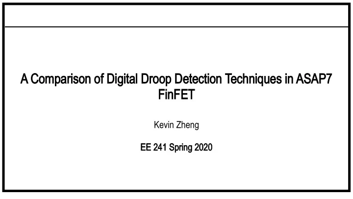
A C Com ompar ariso ison n of D f Dig igita tal D Droop op Dete tecti ction n Tech chni niques i es in ASAP AP7 FinFET Kevin Zheng EE 241 Spring 2020 Out Outli line Motivation Project topic and state of art NAND
A C Com ompar ariso ison n of D f Dig igita tal D Droop op Dete tecti ction n Tech chni niques i es in ASAP AP7 FinFET Kevin Zheng EE 241 Spring 2020
Out Outli line ● Motivation ● Project topic and state of art ● NAND divider and ring oscillator droop detector, design methodology ● Design example and results in ASAP7 ● Conclusion
Th The e Need d For For D Droo oop D Dete tecto ctors ● Power supply challenges of modern systems: – Scaling: more logic density, power consumption – Power gating: large current spikes – System and packaging limit achievable R’s and L’s ● Fast droop detectors required for system performance and reliability
Sta tate te Of Of Ar Art ● Droop detector circuits: mixed-signal and fully-digital ● Part of overall system droop mitigation strategy ● Secondary treatment in existing literature ● Studied in isolation in separate process technologies ● Th This is wo work: compare different fast single-cycle droop detectors in the same technology for the same design specifications
Droo oop D Det etecti ction on Techn chnique ue: : NAND D Divi ivide der Dete tecto ctor ● Analog circuit in disguise ● Voltage divider (NAND gate) followed by comparator (inverter) ● Requires 2-terminal AC-coupling capacitor ● Requires separate, stable AVDD
Desi sign gn Meth thodol ology: N NAND D Divi ivide der Detecto ector ● Input high-pass network – C and W(INV) set input high-pass pole – Set low enough to capture the lowest droop frequency of interest ● Inverter chain – Minimize delay between high-pass node and latch ● Output latch – Any reasonable asynchronous latch
Droop D Detect ectio ion Tech echniqu que: : Ring ng Osc Oscilla lato tor Detecto ector ● Ring oscillator frequency changes instantaneously with VDD ● Use ring oscillator frequency as a measurement of voltage ● Frequency counter with programmable comparator threshold detects droops ● Fully synthesizable
Desig sign M Met ethod odolog ogy: y: Ring g Oscil Oscilla lator or D Dete tect ctor or ● Ring oscillator stages (N) – Pick N, simulate T min – ● Counter threshold (M) – – Account for worse-case corners
Desi sign gn Exa Example les i s in ASA SAP7 ● Fast Design Example – Hypothetical high-performance desktop or server processor – Maximum boost frequency of 4 GHz – Half period: 125 ps ● Slow Design Example – Hypothetical low-power embedded or mobile processor – Core frequency of 800 MHz – Half period: 625 ps
Results ts ● NAND divider detector Design Metric NAND Divider Ring Oscillator – Performs nearly 3x better in all Min. Detectable 38 38 106 measured metrics Droop (mV) – Not fully synthesizable Temp. Sensitivity 110 0 360 / 450 (uV/K) ● Chosen design metrics penalize ring oscillator detector for its Proc. Sensitivity 2 7.4 / 1.9 (mV) process variability Fully No Yes es Synthesizable
Con oncl clusi usion ons ● Topology should be chosen according to specifications and design space exploration ● Design methodologies and automated generators help! ● For these specifications in ASAP7, NAND detector wins on performance
Qu Questio ions? s?
Ref eferences ● [1] J. Crossley et al., "BAG: A designer-oriented integrated framework for the development of AMS circuit generators," 2013 IEEE/ACM International Conference on Computer-Aided Design (ICCAD), San Jose, CA, 2013, pp. 74-81. ● [2] K. L. Wong, T. Rahal-Arabi, M. Ma and G. Taylor, "Enhancing microprocessor immunity to power supply noise with clock-data compensation," in IEEE Journal of Solid-State Circuits, vol. 41, no. 4, pp. 749-758, April 2006. ● [3] J. Oh et. al, "A 480mA Output-Capacitor-Free Synthesizable Digital LDO Using CMP-Triggered Oscillator and Droop Detector with 99.99% Current Efficiency, 1.3ns Response Time, and 9.8A/mm 2 Current Density," ISSCC 2020. ● [4] Y. D. Kim et. al, "A 7nm High-Performance and Energy-Efficient Mobile Application Processor with Tri-Cluster CPUs and a Sparsity-Aware NPU," ISSCC 2020. ● [5] S. Bang et. al, "A Fully Synthesizable Distributed and Scalable All-Digital LDO in 10nm CMOS," ISSCC 2020. ● [6] J. Tschanz, K. Bowman, S. Walstra, M. Agostinelli, T. Karnik and V. De, "Tunable replica circuits and adaptive voltage-frequency techniques for dynamic voltage, temperature, and aging variation tolerance," 2009 Symposium on VLSI Circuits, Kyoto, Japan, 2009, pp. 112-113. ● [7] X. Sun et. al, "A Combined All-Digital PLL-Buck Slack Regulation System with Autonomous CCM/DCM Transition Control and 82% Average Voltage-Margin Reduction in a 0.6-to-1.0V Cortex-M0 Processor," ISSCC 2018. ● [8] H. Mair et. al, "A 7nm FinFET 2.5GHz/2.0GHz Dual-Gear Octa-Core CPU Subsystem with Power/Performance Enhancements for a Fully Integrated 5G Smartphone SoC," ISSCC 2020. ● [9] P. Chiu, M. Ker, "Metal-layer capacitors in the 65 nm CMOS process and the applicationfor low-leakage power-rail ESD clamp circuit," Journal of Microelectronics Reliability, 2014.
Recommend
More recommend
Explore More Topics
Stay informed with curated content and fresh updates.
