SLIDE 1 20
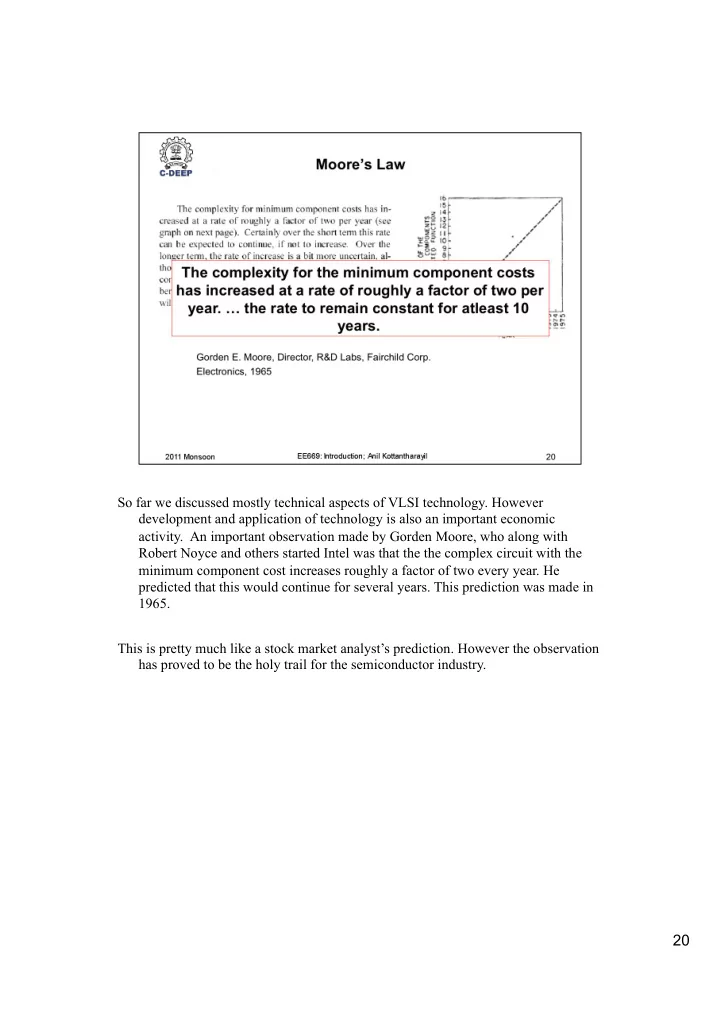
So far we discussed mostly technical aspects of VLSI technology. However development and application of technology is also an important economic
- activity. An important observation made by Gorden Moore, who along with
Robert Noyce and others started Intel was that the the complex circuit with the minimum component cost increases roughly a factor of two every year. He predicted that this would continue for several years. This prediction was made in 1965. This is pretty much like a stock market analyst’s prediction. However the observation has proved to be the holy trail for the semiconductor industry.
SLIDE 2
21
The semiconductor industry has taken the prophecy of Gorden Moore seriously as you can see on this slide. This slide shows the number of transistors per chip for various categories of integrated circuits. You can see that the number of transistors per chip has increased from about 10 in early 1960’s to several billions by 2010. 8 orders of magnitude increase.
SLIDE 3 22
What are the motivations for this dramatic increase in integration density. More complex circuits can be integrated on a single chip. So we have a whole mobile communication system on a chip and there are several such examples. It is increasingly viable to integrate whole electronic systems on a single chip. The speed of devices have increased. The figure shows that every year the instruction processing rate of microprocessors have increased many fold since the early microporcessor. So the performance increase is a very important motivation. The cost has decreased dramatically. We had seen earlier that the early transistors were as expensive as 150 dollars. In today’s cost i.e. 1000 $ ~ Rs 45000. By 2001 that has fallen to 0.00005 Rs. This has also made complex electronic systems affordable to large number of people with a significant improvement in the quality of
- life. In the early stages of transistor electronics, military and space were the main
users of electronic equipment. These are linked to protection of nation states and their pride and no one counted the money spent on these.
SLIDE 4 Title FirstName LastName – Activity / Group 23
- 1. ENIAC made at the University of Pennsylvania in 1946 by John Mauchly
and Presper Eckert for US army ordnance. Used in second world war for calculation of missile projectile tables.
- 2. It was thought of as the first electronic computer till 1973.
- 3. This fascinating success story in engineering, which had a decisive
impact on the way we live also has a fascinating science and technology behind it. This is represented by the devices within these contrasting systems.
- 4. The left hand side shows the picture of a vacuum tube. 18000 of them
were inside one of those early machines. You could hold 10 of them in your palm. The transistor based systems, the whole of it, can be held in your hand.
SLIDE 5
24
The complexity of the electronics industry also grew with complex circuits. This slide shows a snapshot of various sub – industries of the electronic system market and the interplay between them. We will learn how VLSI circuits are fabricated. However you need equipment for manufacturing the circuits, you need a design of the circuit, you need tools for designing circuits, what ever you manufacturer should be tested to specification, an so on. It is not possible for monolithic companies to manage such divergent activities. However the activities must be coordinated for the whole industry to work. For example, a IC manufacturing company decide to come to the market with ICs containing 10nm wide features. The company must have equipment to produce this, equipment to measure such features and also a market where such Ics would find applications. So doing it alone would not help. One of the reason is the cost involved.
SLIDE 6
25
SLIDE 7
26
SLIDE 8
27
This slide shows the global semiconductor industry revenues since 1987. The semiconductor industry contributes 0.6 % of the world’s GDP. In india, that is less than 0.01%. On the other hand the recent estimates suggests that by 2020 our electronic component import would exceed our oil bill. A very unsustainable scenario. WSTS: World semiconductor trade statistics SEMI:
SLIDE 9
28
SLIDE 10
29
SLIDE 11
30
SLIDE 12
31
SLIDE 13
32
SLIDE 14
33
SLIDE 15
34
SLIDE 16 35
In the previous module where we had a peep at the history of the semiconductor engineering, we had seen an example of the transistor assembly line of late 1950’s and early 1960’s. However the yield, the devices or parts those functioned as per specification as a percentage of all the devices or parts made in the same processing lot, was quite low. Junctions made in those days had high leakage currents. Instability in device behavior had delayed the commercial exploitation of
- MOSFETs. The low yield, to a large extent could be attributed to contamination of the wafers during
preparation, during processing and/or during packaging. Contaminant can be defined as any material, the presence of which on the surface or in surface layers or in the bulk of the semiconductor that can result in a reduction in manufacturing yield. Contaminants can be particles from the environment that settle on the surface of the wafers during handling and processing or materials that can be incorporated in the device structures and the bulk
- f the semiconductor. We would review some of the implications of the presence of contaminants on
VLSI technology.
SLIDE 17
36
We would deliberate the impact of particulate contamination on VLSI manufacturing using gate patterning process in CMOS technology. The bottom left figure shows the top view of the wafer after etch of the poly Si and removal of the resist.
SLIDE 18
37
Let us say we want to make several such devices on the wafer. We would connect them together as per the circuit requirements to create an integrated circuit. This is how it should look after gate etch.
SLIDE 19
38
The first process is the photo exposure of the resist. Suppose a particle falls on the resist during the handling of the wafer. The particle, if opaque to the light used for exposure, would block the light from reaching the underlying resist.
SLIDE 20
39
As a result, after development, the resist would look like this.
SLIDE 21
40
The contaminant particle has caused a short between several gates and if the circuit design does not require this, we would have an integrated circuit that would not work. This can happen in any lithography process. Particulate contamination can also be fatal for the IC if it happens during gate oxidation, thin film deposition etc. The IC is likely to work satisfactorily if the size of the particle is smaller than the minimum feature sizes in the IC. More over there may be some parts of the circuit where the features are larger than the smallest, or which contain non critical sections of the circuit etc. These considerations imply that the yield of ICs can be improved by reducing the particle count in the environment in which the ICs are manufactured. With ever decreasing feature sizes in ICs, particle contamination control is very important in semiconductor manufacturing to obtain high yield. Lithography places the highest demands on the particle control, mainly dictated by the fact that feature sizes are decided by lithography processes. A typical state of the art chip fabrication process may involve 30+ lithographic processes.
SLIDE 22 41
The figure shows the simplified band structure of Si and various energy levels in the forbidden gap introduced by impurities in Si. You may learn more about the physics
- f this in the device courses. You may note the energy levels introduced by the
commonly used dopants for controlling conductivity. The defect levels at the middle
- f the bandgap are very efficient in generation and recombination processes.
It suffice to know that the carrier life time, the average time that a carrier is “alive” in the semiconductor, in the case of Si depends inversely on the density of traps, Nt. Let us say we have Au in Si. Nt ~ concentration of Au.
SLIDE 23
42
SLIDE 24 43
MOS structure is the heart of the MOSFET and it consist of a metal gate, insulator (Silicon dioxide) and Silicon. The field effect transistor is highly sensitive to any charges near the surface. Mobile ions in the dielectric can move around in the
- semiconductor. This would cause a shift in the capacitance – voltage characteristics
- f the MOS capacitor (shown) and a corresponding shift in the threshold voltage of
the MOSFET. ΔVt = -QM/COX Where QM is the mobile charge density in Coulomb per cm2 and COX is the oxide capacitance per cm2.
SLIDE 25
44