SLIDE 1
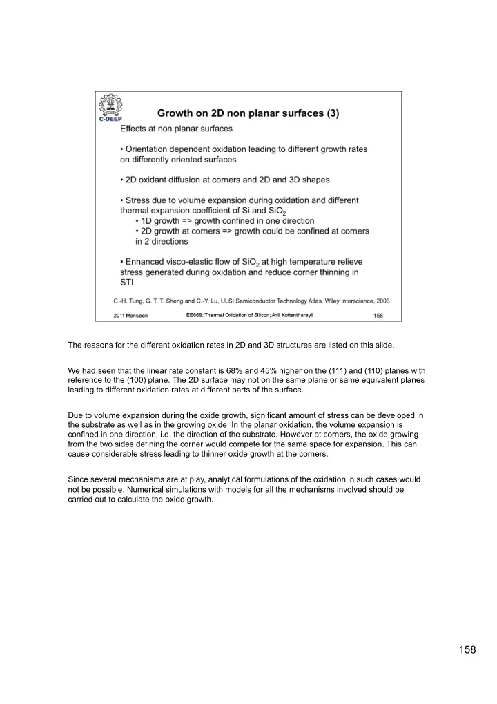
The reasons for the different oxidation rates in 2D and 3D structures are listed on this slide. We had seen that the linear rate constant is 68% and 45% higher on the (111) and (110) planes with reference to the (100) plane. The 2D surface may not on the same plane or same equivalent planes leading to different oxidation rates at different parts of the surface. Due to volume expansion during the oxide growth, significant amount of stress can be developed in the substrate as well as in the growing oxide. In the planar oxidation, the volume expansion is confined in one direction, i.e. the direction of the substrate. However at corners, the oxide growing from the two sides defining the corner would compete for the same space for expansion. This can cause considerable stress leading to thinner oxide growth at the corners. Since several mechanisms are at play, analytical formulations of the oxidation in such cases would not be possible. Numerical simulations with models for all the mechanisms involved should be carried out to calculate the oxide growth.
158
SLIDE 2
SiO2 can experience visco-elastic flow at high temperature. Viscosity is the resistance shown by a liquid to deformation. For example, honey has higher viscosity than water and would not flow as easily as water. The viscosity of glasses, including pure SiO2 decreases with increasing temperature. This can be used for relieving stresses at corners, i.e. by carrying out oxidation at high temperatures, the corner effect we have discussed in relation to STI process can be reduced. In a previous lecture we had seen that oxidation in a wet ambient would result in a weakening of the SiO2 by the formation of Si-OH bonds. This could result in easier flow of the SiO2 formed. Wet oxidation may be preferred for corner rounding applications.
159
SLIDE 3
160
SLIDE 4 By non local, we mean oxidation induced effects far from the interface at which the
- xidation reaction is happening. These cannot be explained by the macroscopic
model we have used extensively to develop an understanding of the process so far. The macroscopic model is concerned with the diffusion through the growing oxide and the reaction at the interface. However it is seen that surface oxidation can also modify dopant profiles deep in the silicon. An important aspect that was discussed earlier during the module on crystal growth was that SiO2 growth involve volume expansion and the additional volume can be created by absorbing vacancies and generating interstitials. The vacancies diffuse to the surface from the silicon crystal and the interstitials can be injected into the
- crystal. These could enhance or retard diffusion of dopants already present in the
wafer. We will study the impact of point defects on diffusion in the module on diffusion.
161
SLIDE 5
Higher vacancy concentration would help relax the strain due to volume expansion and this could speed up the interface reaction. However this would be a deciding factor mainly in the linear regime of growth.
162
SLIDE 6 163
This is a recap of what we had previously discussed regarding point defects. The concentration of neutral vacancies, CV0 and interstitials, CI0 are given as a function
- f temperature. The concentration would increase with temperature.
The energy of the electronic states introduced by charged states in the forbidden energy gap of silicon are also shown.
SLIDE 7 164
While using various numbers given in these slides or those given in books you should be careful about the assumption of accuracy. This particular slide shows the equilibrium vacancy concentration in Silicon as a function of temperature reported by different authors in the literature. The solid lines are from theoretical estimates and the dashed line is experimental fit to diffusion data. Various theoretical models proposed by various authors differ in their estimates by several orders of magnitude. Note that experimental data from only one source is given in this figure. The accuracy of the data would indeed depend on the accuracy of the theoretical model used to describe the diffusion process in terms of processes involving point defects. The true test of a model is to accurately describe experimental observations, not only qualitatively but also quantitatively. Many scenarios can be discussed in this context: (i) The model may not take into account all the physical phenomenon involved (ii) The experiment is not carefully carried out in the sense that several secondary effects come into the picture (iii) The model may be derived based
- n wrong assumptions or wrongly understood physics of the problem……..
SLIDE 8
165
The concentrations of charged vacancies are shown on this slide. The prefactor CV0 increases with temperature as was discussed on the previous slide. The position of the defect state relative to the fermi level is decisive. The fermi level is at the middle of the bandgap when the material is intrinsic. The intrinsic carrier concentration depends on the temperature. The consequence is that the material is intrinsic when ni > |NA – ND|.
SLIDE 9 166
T is the temperature in Kelvin, k is the Boltzmann constant and EG is the bandgap. Bandgap also shows a dependence on temperature. Let us take a Silicon wafer with n-type doping of 1016 cm-3. The material would be a n-type semiconductor till a temperature of 500 C beyond which it would be intrinsic. Similarly a 2 x 1018 cm-3 n-type doped Si would be n-type till a temperature of 1000 C, beyond which it would be an intrinsic semiconductor. Or in other words, for a processing temperature of 1000 C, for doping concentrations below 2 x 1018 cm-3 the semiconductor would be intrinsic and above this doping concentration, the semiconductor would be extrinsic. For an intrinsic material, the fermi level would be at the middle of the band gap. For an n-type material, the fermi level would be closer to the conduction band. For a p-type material, the fermi level would be closer to the valance band. Based on this discussion and the equations seen on the previous slide, it is obvious that the density
- f charged point defects would depend on the temperature as well as the type and level of the
doping of the semiconductor.
SLIDE 10
167
The vacancy concentrations calculated for 4 different cases at 850 C is shown on the slide. It is seen that the n-type silicon with 5 x 1019 cm-3 doping has the highest total concentration of vacancies. It can be expected that the heavily n-type doped silicon would oxidize faster than the other cases. The temperature dependence of band gap was not taken into account in the calculations shown.
SLIDE 11
168
SLIDE 12
169
SLIDE 13
170
SLIDE 14
171