0D, 1D, and 2D Structures Clusters, Nanowires, Graphene CINT/JAIST - - PowerPoint PPT Presentation

0d 1d and 2d structures clusters nanowires graphene
SMART_READER_LITE
LIVE PREVIEW

0D, 1D, and 2D Structures Clusters, Nanowires, Graphene CINT/JAIST - - PowerPoint PPT Presentation

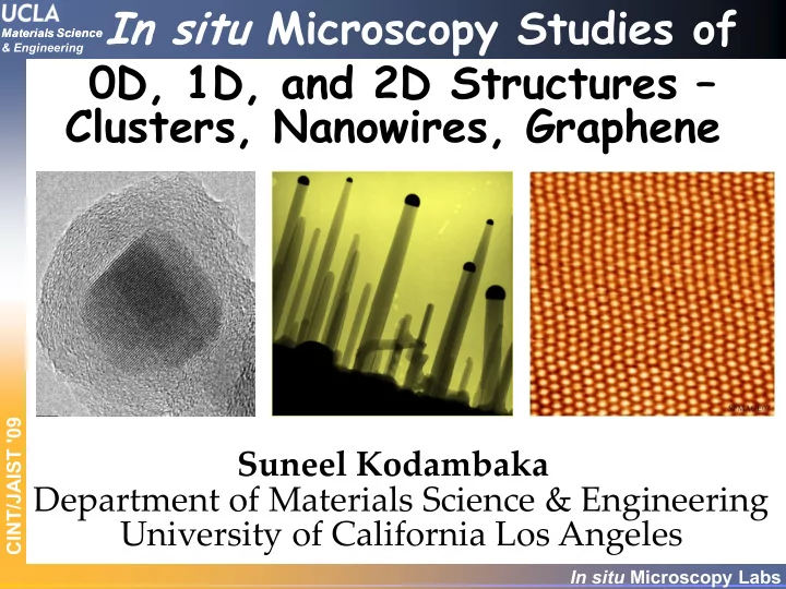
In situ Microscopy Studies of Materials Science Materials Science & Engineering 0D, 1D, and 2D Structures Clusters, Nanowires, Graphene CINT/JAIST '09 Suneel Kodambaka Department of Materials Science & Engineering University of


slide-1
SLIDE 1

CINT/JAIST '09

Materials Science & Engineering Materials Science

In situ Microscopy Labs

In situ Microscopy Studies of 0D, 1D, and 2D Structures – Clusters, Nanowires, Graphene

Suneel Kodambaka Department of Materials Science & Engineering University of California Los Angeles

slide-2
SLIDE 2

CINT/JAIST '09

Materials Science & Engineering Materials Science

  • 3. Growth of Semiconducting Graphene
  • n Pd(111)

height (Å) 22 Å Pd[110] Gr[2110] 40 nm C D A B 10 nm X X' O X X' O distance (Å)

50 100 150 200 0.05 0.10 0.15 0.20

Questions we'd like to address: 1.How does graphene form? 2.What is the role of substrate?

Potentially transformative Can be tailor the electronic properties of epitaxial graphene & grow "device-ready" layers on Si wafers?

slide-3
SLIDE 3

CINT/JAIST '09

Materials Science & Engineering Materials Science

Graphene/Pd(111): tunneling bias-dependent image contrast

I = 0.24 nA VT = +1.1 V = +1.1 V I = 0.24 nA VT = = -1.1 V 1.1 V

slide-4
SLIDE 4

CINT/JAIST '09

Materials Science & Engineering Materials Science

band gap of 0.2-0.3 eV!

STS of Graphene/Pd(111)

  • 2.0
  • 1.5
  • 1.0
  • 0.5

0.0 0.5 1.0 1.5 2.0 2 4 6 8 10

  • 2
  • 1

1 2 1 2 3 4 5 6 7 (dI/dV) / (I/V) V (V)

8.3 nm

  • 0.4 -0.2

0.0 0.2 0.4 1 2

(dI/dV)/(I/V)

0.25eV

  • 6
  • 4
  • 2

2 4 6 2 4 6 8 10 12 14 16

PDOS

E (eV)

LDOS

0.25 eV 0.3 eV

STM DFT

Substrate can greatly influence graphene properties

slide-5
SLIDE 5

CINT/JAIST '09

Materials Science & Engineering Materials Science

In situ Microscopy Labs

  • 2. Nucleation and Growth Kinetics
  • f Si and Ge nanowires
  • J. Tersoff, M.C. Reuter, and F.M. Ross

IBM T. J. Watson Research Center, Yorktown Heights B.-J. Kim, C.-Y. Wen, and E.A. Stach

  • Dept. Materials Science and Engineering, Purdue University

Partially funded by UC Discovery, UCEI, & Northrop Grumman Space Technology Questions we'd like to address: 1.How do nanowires grow? 2.What is the role of catalyst composition?

Potentially transformative Can be fabricate nanowire heterostructures with atomically abrupt interfaces, tunable shapes & structures?

slide-6
SLIDE 6

CINT/JAIST '09

Materials Science & Engineering Materials Science

T = 525 oC; Si2H6 = 8 10-7 Torr Crystalline Au + Si2H6 → liquid AuSi droplets → Si nw/AuSi t = 0, vacuum

Si wire nucleation kinetics

slide-7
SLIDE 7

CINT/JAIST '09

Materials Science & Engineering Materials Science

Si wire nucleation kinetics

t=226 s t=233 s t=390 s T = 525 oC Si2H6: 410-6 Torr

500 600 700 800 3 4 5 6

t (sec) r (nm)

C

Rapid initial growth crossover to slow growth Critical supersaturation of Si in AuSi droplets

 

1 LS

k c d c r dt  

 

3 1 VL LS

P r k t t k R R          

B.J. Kim, J. Tersoff, S. Kodambaka, M.C. Reuter, E.A. Stach, & F.M. Ross, Science 322, 1070 (2008).

slide-8
SLIDE 8

CINT/JAIST '09

Materials Science & Engineering Materials Science

tmovie: 30x texpt wire diameter: 25 nm 90 nm Ge nanowire morphology can be controllably manipulated with deposition pressures T = 410 oC

Ge wire growth vs. Ge2H6 flux

slide-9
SLIDE 9

CINT/JAIST '09

Materials Science & Engineering Materials Science

In situ Microscopy Labs

  • 1. Thermal/Chemical Stability of

Small Clusters

Funded by ACS-PRF 48108-G10 & Hitachi Labs Questions we'd like to address: 1.How do hollow core structures form? 2.What is the role of surface/interface structure & orientation? 3.What controls their stability?

Potentially transformative Can be make better & cheaper catalysts?

slide-10
SLIDE 10

CINT/JAIST '09

Materials Science & Engineering Materials Science

T = 850ºC 10 s 236 s 241 s 900 s 1022 s 1023 s 1024 s

Ostwald ripening of the titania cores

Larger TiO2 core grows at the expense of smaller one resulting in hollow graphitic shells At longer times, only hollow cores remain.

slide-11
SLIDE 11

CINT/JAIST '09

Materials Science & Engineering Materials Science

In situ SEM studies of: * Nanowire nucleation & growth kinetics * Liquid droplet/solid surface dynamics * Chemical & thermal stabilities of nanostructures

Ultra Ultra-

  • High Vacuum Variable

High Vacuum Variable-

  • Pressure

Pressure Scanning Electron Microscope Scanning Electron Microscope

UHV-CVD in a SEM: Operating pressure:10-7 – 1 mTorr Temperatures:

300 - 1250 K

Imaging modes: SE, BSE, STEM

Funded by Dept. Materials Science & School of Engineering at UCLA