
SLIDE 1
16.1
Unit 16
Computer Organization and Instruction Sets
16.2
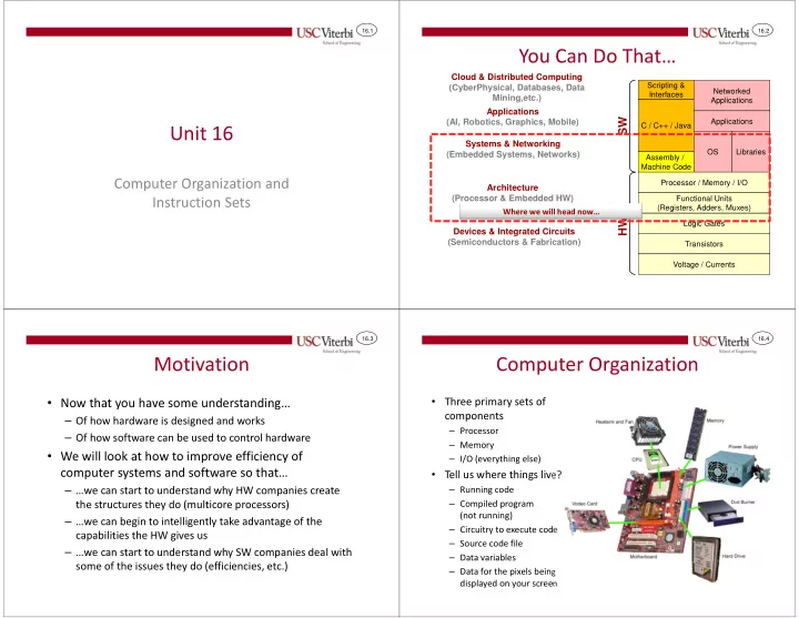
You Can Do That…
C / C++ / Java Logic Gates Transistors
HW SW
Voltage / Currents Assembly / Machine Code Applications Libraries OS Processor / Memory / I/O Functional Units (Registers, Adders, Muxes)
Devices & Integrated Circuits (Semiconductors & Fabrication) Architecture (Processor & Embedded HW) Systems & Networking (Embedded Systems, Networks) Applications (AI, Robotics, Graphics, Mobile) Cloud & Distributed Computing (CyberPhysical, Databases, Data Mining,etc.)
Scripting & Interfaces Networked Applications
Where we will head now…
16.3
Motivation
- Now that you have some understanding…
– Of how hardware is designed and works – Of how software can be used to control hardware
- We will look at how to improve efficiency of
computer systems and software so that…
– …we can start to understand why HW companies create the structures they do (multicore processors) – …we can begin to intelligently take advantage of the capabilities the HW gives us – …we can start to understand why SW companies deal with some of the issues they do (efficiencies, etc.)
16.4
Computer Organization
- Three primary sets of
components
– Processor – Memory – I/O (everything else)
- Tell us where things live?
– Running code – Compiled program (not running) – Circuitry to execute code – Source code file – Data variables – Data for the pixels being displayed on your screen