
SLIDE 1
VLSI Design Verification and Test Defects CMPE 646 1 (9/28/04)
UMBC
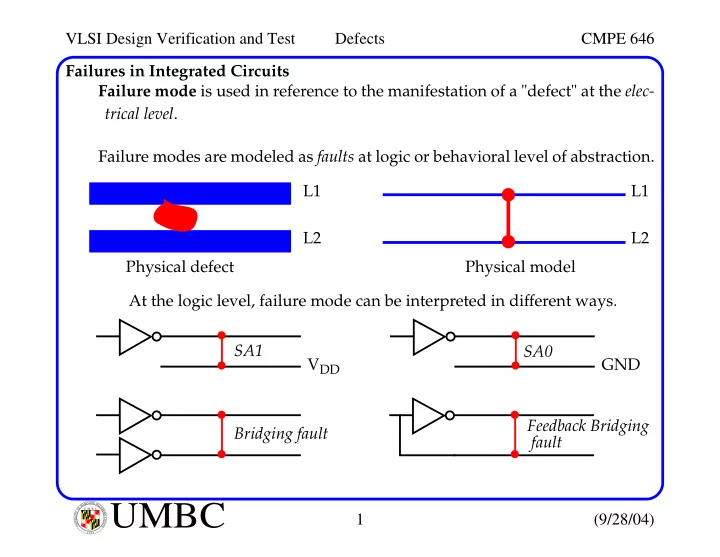
U M B C U N I V E R S I T Y O F M A R Y L A N D B A L T I M O R E C O U N T Y 1 9 6 6Failures in Integrated Circuits Failure mode is used in reference to the manifestation of a "defect" at the elec- trical level. Failure modes are modeled as faults at logic or behavioral level of abstraction. L1 L2 L1 L2 Physical defect Physical model VDD At the logic level, failure mode can be interpreted in different ways. GND SA1 SA0 Bridging fault Feedback Bridging fault