
SLIDE 1
Systems Design and Programming Basic I/O I CMPE 310 1 (April 1, 2002)
UMBC
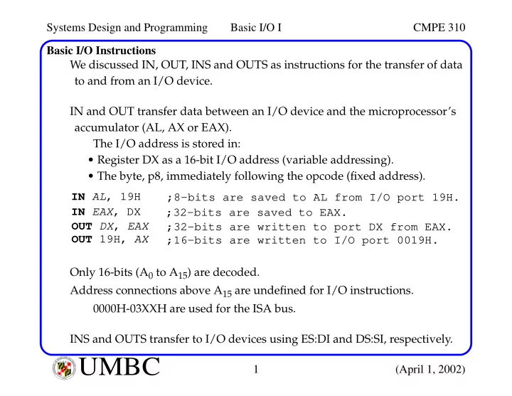
U M B C U N I V E R S I T Y O F M A R Y L A N D B A L T I M O R E C O U N T Y 1 9 6 6Basic I/O Instructions We discussed IN, OUT, INS and OUTS as instructions for the transfer of data to and from an I/O device. IN and OUT transfer data between an I/O device and the microprocessor’s accumulator (AL, AX or EAX). The I/O address is stored in:
- Register DX as a 16-bit I/O address (variable addressing).
- The byte, p8, immediately following the opcode (fixed address).
Only 16-bits (A0 to A15) are decoded. Address connections above A15 are undefined for I/O instructions. 0000H-03XXH are used for the ISA bus. INS and OUTS transfer to I/O devices using ES:DI and DS:SI, respectively. IN AL, 19H ;8-bits are saved to AL from I/O port 19H. IN EAX, DX ;32-bits are saved to EAX. OUT DX, EAX ;32-bits are written to port DX from EAX. OUT 19H, AX ;16-bits are written to I/O port 0019H.