umbc
play

UMBC A B M A L T F O U M B C I M Y O R T 1 - PowerPoint PPT Presentation

Digital Systems Crosstalk I CMPE 650 Crosstalk Ground and power planes serve to: Provide stable reference voltages Distribute power to logic devices Control crosstalk Here, we derive formulas for computing crosstalk and show how


  1. Digital Systems Crosstalk I CMPE 650 Crosstalk Ground and power planes serve to: • Provide stable reference voltages • Distribute power to logic devices • Control crosstalk 
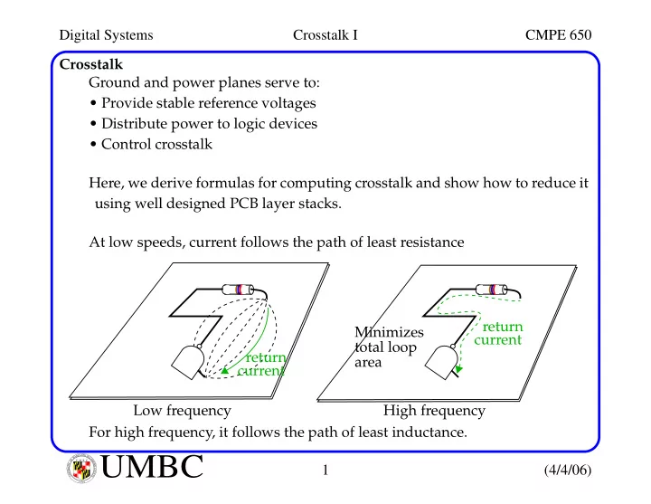
Here, we derive formulas for computing crosstalk and show how to reduce it using well designed PCB layer stacks. At low speeds, current follows the path of least resistance return Minimizes current total loop return area current Low frequency High frequency For high frequency, it follows the path of least inductance. L A N R Y D UMBC A B M A L T F O U M B C I M Y O R T 1 (4/4/06) I E S R C E O V U I N N U T Y 1 6 9 6

  2. Digital Systems Crosstalk I CMPE 650 Crosstalk The return current distribution: Cross section of PCB W Current density Signal trace H Ground D I 0 Current density for a 1 ( ) ⁄ i D - A in. = - - - - - - - - - - - - - - - - - - - - - - - - - - - - - - - - - - - - - point D inches away π H ) 2 ( ⁄ D H 1 + from trace. Here, we see a balance between two opposing forces. Too narrow a distribution increases inductance (skinny wires have more inductance than broad ones) and too broad a distribution increases inductance (by increasing loop area). The real distribution minimizes inductance. The current distribution given by this equation also minimizes the total energy stored in the magnetic field surrounding the signal wire. L A N R Y D UMBC A B M A L T F O U M B C I M Y O R T 2 (4/4/06) I E S R C E O V U I N N U T Y 1 6 9 6

  3. Digital Systems Crosstalk I CMPE 650 Crosstalk in Solid Ground Planes Crosstalk depends on the amount of mutual inductance and capacitance. We focus on inductive crosstalk since it is usually as big or bigger than capacitive crosstalk in digital systems. We covered the theory of mutual inductance coupling earlier. Returning signal currents generate magnetic fields, which induce volt- ages in other circuit traces. The induced voltages are proportional to the derivative of the driving sig- nal, e.g., faster rise times produce a more significant effect. Signal traces H Ground D Ratio of measured noise voltage and driving step size K where K depends on the rise time Crosstalk = - - - - - - - - - - - - - - - - - - - - - - - - - - - - - - ) 2 and length of interfering traces (<1). ( ⁄ D H 1 + L A N R Y D UMBC A B M A L T F O U M B C I M Y O R T 3 (4/4/06) I E S R C E O V U I N N U T Y 1 6 9 6

  4. Digital Systems Crosstalk I CMPE 650 Crosstalk in Solid Ground Planes Experiment to test the D/H dependency in this equation. Each trace cross section 26 in. long 0.020 H E r = 4.5 D Height can 0.080 be varied Here, the height H can be changed by adding dielectric plates. 50 3.6V step Mutual H 20 inductance (nH) 10 200 see txt 0.010 5 area method for others mV/div 2 no GND plane D/H 1 2 5 10 10 ns/div L A N R Y D UMBC A B M A L T F O U M B C I M Y O R T 4 (4/4/06) I E S R C E O V U I N N U T Y 1 6 9 6

  5. Digital Systems Crosstalk I CMPE 650 Crosstalk in Slotted Ground Planes Slotted GND planes are a big mistake: Large loop increases Hole in GND plane For connectors inductance and BAD GOOD increases rise time A B of signal at B . Overlap with C-D return current D increases mutual C inductance. You may be tempted to do this when you run out of room on the regular routing layers and cram a trace in on the GND plane. The effective inductance in series with A-B is approximated by: D = perpendicular extent of current diversion D   L 5 D - - - - - = ln away from signal trace, in.   W W = trace width, in. Inductance is almost completely independent of slot width , i.e., making the slot narrow does NOT help. L A N R Y D UMBC A B M A L T F O U M B C I M Y O R T 5 (4/4/06) I E S R C E O V U I N N U T Y 1 6 9 6

  6. Digital Systems Crosstalk I CMPE 650 Crosstalk in Slotted Ground Planes Rise time degradation depends on the termination conditions. The worse case is a long line with an apparent src resistance on either side of the inductance of Z 0 . The resulting 10-90% rise time of the L/R filter (weighted in with the natural signal rise time) is: 2.2 L T 10-90 L/R ) 2 ) 2 = - - - - - - - - - ( ( T composite T 10-90 L/R T 10-90 signal = + 2 Z 0 For a short line driving a heavy capacitive load C , the 10-90% rise time (assuming critical damping) is: T 10 3.4 LC = – 90 The Q of this circuit depends on R S . If Q > 1, it rings, if Q is near 1, this equation approximates rise time well, if Q < 1, the rise time is actually slower than this approximation. L A N R Y D UMBC A B M A L T F O U M B C I M Y O R T 6 (4/4/06) I E S R C E O V U I N N U T Y 1 6 9 6

  7. Digital Systems Crosstalk I CMPE 650 Crosstalk in Slotted Ground Planes If a second trace, e.g. C-D also intersects the slot, the mutual inductance between the two traces is given by the previous inductance formula. The cross coupling voltage is derived by the mutual inductance and the time rate of change in current in the driver. ∆ I V crosstalk - L M - - - - - - - - - - - - - - - = T 10-90 For a long line, the ∆ I is the drive voltage/ characteristic impedance . ∆ V V crosstalk - L M - - - - - - - - - - - - - - - - - - - - - - = T 10-90 Z 0 For short lines driving a large capacitive load, the time rate of change in cur- rent is the second derivative of voltage: 1.52 ∆ VC V crosstalk - L M - - - - - - - - - - - - - - - - - - - - - - - = ) 2 ( T 10-90 L A N R Y D UMBC A B M A L T F O U M B C I M Y O R T 7 (4/4/06) I E S R C E O V U I N N U T Y 1 6 9 6

  8. Digital Systems Crosstalk I CMPE 650 Crosstalk in Cross-Hatched Ground Planes If you are forced to use a two layer board: By-pass caps Top Bottom layer layer Returning current must follow power and ground wires to stay close to outgoing signal path. V DD GND Note that signals are interleaved with the power and GND routing. This layout increases mutual inductance . Appropriate for low-speed CMOS and TTL design -- not high-speed logic. Current returns equally well through the GND and power wires. L A N R Y D UMBC A B M A L T F O U M B C I M Y O R T 8 (4/4/06) I E S R C E O V U I N N U T Y 1 6 9 6

  9. Digital Systems Crosstalk I CMPE 650 Crosstalk in Cross-Hatched Ground Planes Will your circuit work with the increased mutual inductance (over solid GND planes )? First estimate the self-inductance : X X = hatch width, in.   ≈ L 5 Y - - - - - ln   W = trace width, in. W Y = trace length, in. Here, trace length is the directed distance between the src and driver. This equation can also be used to estimate the mutual inductance , L M , for a 2nd trace that runs closely to the first. If two traces are separated by a larger distance D , the mutual inductance decreases, modeled with D in the denominator as before: ( ⁄ ) 5 Y X W ln L M = - - - - - - - - - - - - - - - - - - - - - - - - - - - - - - - ) 2 ( ⁄ D X 1 + Rise time degradation and cross-talk voltage computed as before. L A N R Y D UMBC A B M A L T F O U M B C I M Y O R T 9 (4/4/06) I E S R C E O V U I N N U T Y 1 6 9 6

  10. Digital Systems Crosstalk I CMPE 650 Crosstalk with Power and Ground Fingers This scheme saves even more board area: Return current forced to flow Fattening around edge of the power board and GND trace widths does not BAD DESIGN help STYLE Both power and GND are routed on the same layer. The diversion of the current introduces a huge amount of self and mutual inductance , both modeled as . X = board width! X   ≈ L 5 Y ln - - - - - W = trace width   W Y = trace length L A N R Y D UMBC A B M A L T F O U M B C I M Y O R T 10 (4/4/06) I E S R C E O V U I N N U T Y 1 6 9 6

  11. Digital Systems Crosstalk I CMPE 650 Guard Traces These are used a lot in analog design: Grounded Can reduce guard crosstalk by an traces order of magnitude See text for other illustrations Signal trace However, for digital, solid GND planes provide most of the benefits of guard traces (guard traces help very little). As a rule of thumb, coupling between microstrip signal lines is cut in half by inserting a third line (GNDed at both ends) between them. Coupling is halved yet again if the third line is frequently tied (through vias) to the GND plane. In digital with a solid GND plane, the reduction in crosstalk is not significant even if it’s possible to insert a guard trace between two traces. L A N R Y D UMBC A B M A L T F O U M B C I M Y O R T 11 (4/4/06) I E S R C E O V U I N N U T Y 1 6 9 6

Download Presentation
Download Policy: The content available on the website is offered to you 'AS IS' for your personal information and use only. It cannot be commercialized, licensed, or distributed on other websites without prior consent from the author. To download a presentation, simply click this link. If you encounter any difficulties during the download process, it's possible that the publisher has removed the file from their server.

Recommend


More recommend