umbc
play

UMBC L A N R Y D A B M A L T F O U M B C I M Y - PowerPoint PPT Presentation

VLSI Design Verification and TestTest Economics/Yield CMPE 646 Test Economics Engineers concerned with optimizing technological efficiency. Economists prefer to minimize cost. Fixed and variable costs of material, equipment, labor, etc. are


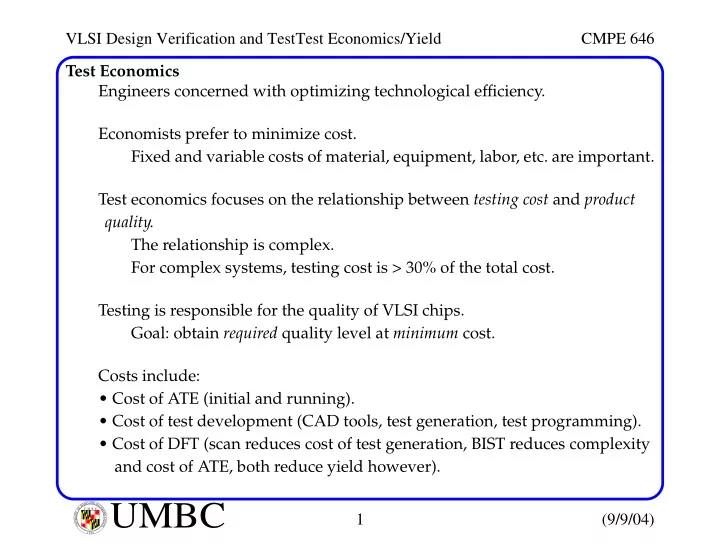
  1. VLSI Design Verification and TestTest Economics/Yield CMPE 646 Test Economics Engineers concerned with optimizing technological efficiency. Economists prefer to minimize cost. Fixed and variable costs of material, equipment, labor, etc. are important. Test economics focuses on the relationship between testing cost and product quality . The relationship is complex. For complex systems, testing cost is > 30% of the total cost. Testing is responsible for the quality of VLSI chips. Goal: obtain required quality level at minimum cost. Costs include: • Cost of ATE (initial and running). • Cost of test development (CAD tools, test generation, test programming). • Cost of DFT (scan reduces cost of test generation, BIST reduces complexity and cost of ATE, both reduce yield however). UMBC L A N R Y D A B M A L T F O U M B C I M Y O R 1 (9/9/04) T I E S R C E O V U I N N U T Y 1 6 9 6
  2. VLSI Design Verification and TestTest Economics/Yield CMPE 646 Yield Process yield : fraction of acceptable parts among all parts fabricated. Wafer yield : average number of good chips/wafer. Normalizing wafer yield by the # of chip sites on the wafer can be used as process yield. Many factors affect yield including die area , process maturity and number of pro- cess steps . It is difficult to obtain an exact value of yield: • Tests are based on fault models that do not detect all defects. • Lack of data once the product is sold. Defect Level ( DL ) are the fraction of bad chips that pass final package tests. DL is usually expressed in Defect-Per-Million or DPM . UMBC L A N R Y D A B M A L T F O U M B C I M Y O R 2 (9/9/04) T I E S R C E O V U I N N U T Y 1 6 9 6

  3. VLSI Design Verification and TestTest Economics/Yield CMPE 646 Defect Modeling Two scenarios for defect modeling: Defects Good chips Bad chips Unclustered defects Clustered defects Wafer yield = 12/22 = 0.55 Wafer yield = 17/22 = 0.77 Fortunately, clustered defect model better represents reality. Random defects are characterized by two parameters: • defect density, d , which is the average number of defects per unit area. • clustering parameter, α . The average number of defects on a chip of area A is Ad . UMBC L A N R Y D A B M A L T F O U M B C I M Y O R 3 (9/9/04) T I E S R C E O V U I N N U T Y 1 6 9 6

  4. VLSI Design Verification and TestTest Economics/Yield CMPE 646 Defect Modeling In any random chip, the number of defects, x , is an integer-valued random variable. Defect clustering is best modeled assuming a negative binomial probability density function for x : ( ) ( ) p x Prob # of defects on chip=x = ) x Γ α ( ) ( Ad α ⁄ x + ( ) p x = - - - - - - - - - - - - - - - - - - - - - - - - - - - - - - - - - - - - - - - - - - - - - - - - - - - - - - - - - - - - - - (1) x ! Γ α ( ) ) α x + ( Ad α ⁄ 1 + where Γ x ( ) is the gamma function given by ∞ – x n e x – 1 Γ x ( ) ∫ d x = 0 The mean, E( x ), and variance, σ 2 x ( ) are defined as: ( ) E x Ad = (1a) σ 2 x ( ) ( Ad α ⁄ ) Ad 1 = + UMBC L A N R Y D A B M A L T F O U M B C I M Y O R 4 (9/9/04) T I E S R C E O V U I N N U T Y 1 6 9 6

  5. VLSI Design Verification and TestTest Economics/Yield CMPE 646 Yield Models In order to predict the yield, we need the mean and variance for the number of defects on a chip. Obtain either from experimental measurements or process simulation. Substitution of the mean and variance in equations (1a) gives yield parame- ters, d and α . Yield is obtained as the probability, p (0), of no defect on a chip. Substituting x= 0 into the equation (1) gives: ) α – ( Ad α ⁄ Y (2) = 1 + For the unclustered model: ) x e Ad – ( Ad α → ∞ ⇒ ( ) p x = - - - - - - - - - - - - - - - - - - - - - - - - - - - x ! e Ad – with x = 0, the yield is: Y Poisson = (3) UMBC L A N R Y D A B M A L T F O U M B C I M Y O R 5 (9/9/04) T I E S R C E O V U I N N U T Y 1 6 9 6

  6. VLSI Design Verification and TestTest Economics/Yield CMPE 646 Yield Models However, this model predicts low yields. If Ad = 1.0 and α = 0.5 (typical of a large VLSI chip) then using (3): 1 Y Poisson = - - - = 0.37 (4) e Using (2), a more realistic prediction of 0.58 is obtained. Yield may be low when fabricating a new design, and more accurately predi- cated by (3) than by (2). Consider the impact of testability (the cost of testability overhead): • d = 1.25 defects/cm 2 • α = 0.5 • chip area, A , is 8mm X 8mm = 0.64cm 2 . Equation (2) gives: ×  0.5 –  0.64 1.25 Y = 1 + - - - - - - - - - - - - - - - - - - - - - - - - - - - = 0.62   0.5 UMBC L A N R Y D A B M A L T F O U M B C I M Y O R 6 (9/9/04) T I E S R C E O V U I N N U T Y 1 6 9 6

  7. VLSI Design Verification and TestTest Economics/Yield CMPE 646 Example Now suppose: • The process uses 8-inch wafers • The cost of processing a wafer is $100 • Each wafer has 400 chips Processing cost per chip is: $100 Cost chip = - - - - - - - - - - - - - - - - - - - - - - - - - - - - - - = 40 cents ( × ) 400 0.62 Assume the chip size increases by 10% after DFT is included. Yield is then: × ×  0.5 –  0.64 1.10 1.25 Y DFT 2% reduction in yield = 1 + - - - - - - - - - - - - - - - - - - - - - - - - - - - - - - - - - - - - - - - - - - - - = 0.60   0.5 With DFT, a wafer contains 400/1.1 ~= 364 chips. Therefore, processing cost is: $100 Cost chip = - - - - - - - - - - - - - - - - - - - - - - - - - - - - - - = 46 cents 15% increase over no DFT ( × ) 364 0.60 UMBC L A N R Y D A B M A L T F O U M B C I M Y O R 7 (9/9/04) T I E S R C E O V U I N N U T Y 1 6 9 6

  8. VLSI Design Verification and TestTest Economics/Yield CMPE 646 DL and Quality DL (or reject ratio) is a measure of the effectiveness of the tests. Objective is to develop a test that reduces the number of outgoing faulty parts to an acceptable level It’s too expensive to try to get them all. The DL can be determined from the field return data. Chips are returned if they fail acceptance test, fail system test or fail in the field during a maintenance test. For commercial VLSI chips, a DL >500ppm is considered unacceptable. Actual DL is difficult to determine: • Some failed parts are not returned • Some returned parts are damaged in handling • It takes a long time (a year) to collect sufficient data • The DL reduces over time Therefore, computed DL is usually overly pessimistic. Test data analysis from manufacturing test data gives estimate. UMBC L A N R Y D A B M A L T F O U M B C I M Y O R 8 (9/9/04) T I E S R C E O V U I N N U T Y 1 6 9 6

  9. VLSI Design Verification and TestTest Economics/Yield CMPE 646 Estimating Defect Level The yield equation (1) can be modified to do this. • Fault density (as opposed to defect density) defined as f = average number of SA faults per unit chip area. • Fault clustering parameter, β • Stuck-At fault coverage, T . ) β – ( ) ( ⁄ β Y T TA f = 1 + Here, we obtain the "measured" yield when a test with fault coverage T is applied. Assume that tests with 100% fault coverage (T=1.0) remove all faulty chips: ) β – (5) ( ) ( ⁄ β Y Y A f = 1 = 1 +  β ( ) ( ) β Y T Y 1 TAf  – + (multiply by 10 6 to ( ) DL T = - - - - - - - - - - - - - - - - - - - - - - - - - - - - - - = 1 – - - - - - - - - - - - - - - - - - - -   ( ) β Y T Af (6) + get PPM). Af (average number of faults) and β are determined from test data. UMBC L A N R Y D A B M A L T F O U M B C I M Y O R 9 (9/9/04) T I E S R C E O V U I N N U T Y 1 6 9 6

  10. VLSI Design Verification and TestTest Economics/Yield CMPE 646 Estimating Defect Level from SEMATECH data This model can be evaluated on IBM’s SEMATECH data. CUT characteristics: • CUT is a bus interface controller ASIC containing 116,000 equivalent 2- input NAND gates. • CUT has 249 I/O and a 304-pin package. • Some portions of chip operate at 40MHz, others at 50MHz. • Full scan, with 5,280 scan latches. • 3.3V power supply, 3 metal, 0.45um technology, 9.4mm x 8.8 mm die size. • Four types of tests applied, SA, functional, delay and I DDQ . IBM’s LSSD scan chain design allows a scan flush test. • With scan tests, total SA coverage was 99.79% for a total of 375,142 faults. • Advantest 3381 ATE used. • 18,466 chips tested at 2.5MHz test clock. (Data provided courtesy Phil Nigh, IBM). UMBC L A N R Y D A B M A L T F O U M B C I M Y O R 10 (9/9/04) T I E S R C E O V U I N N U T Y 1 6 9 6

Download Presentation
Download Policy: The content available on the website is offered to you 'AS IS' for your personal information and use only. It cannot be commercialized, licensed, or distributed on other websites without prior consent from the author. To download a presentation, simply click this link. If you encounter any difficulties during the download process, it's possible that the publisher has removed the file from their server.

Recommend


More recommend