
SLIDE 1
Systems Design and Programming Bus Interface CMPE 310 1 (May 6, 2002)
UMBC
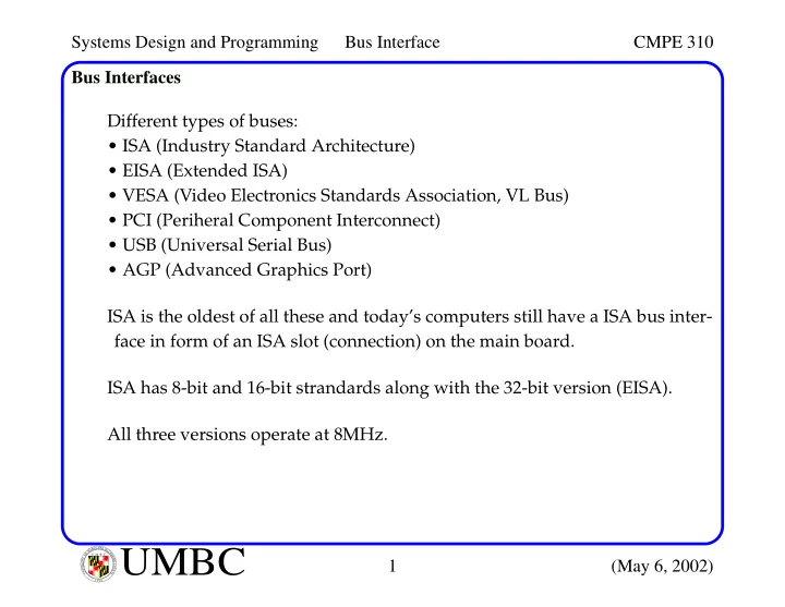
U M B C U N I V E R S I T Y O F M A R Y L A N D B A L T I M O R E C O U N T Y 1 9 6 6Bus Interfaces Different types of buses:
- ISA (Industry Standard Architecture)
- EISA (Extended ISA)
- VESA (Video Electronics Standards Association, VL Bus)
- PCI (Periheral Component Interconnect)
- USB (Universal Serial Bus)
- AGP (Advanced Graphics Port)
ISA is the oldest of all these and today’s computers still have a ISA bus inter- face in form of an ISA slot (connection) on the main board. ISA has 8-bit and 16-bit strandards along with the 32-bit version (EISA). All three versions operate at 8MHz.