umbc
play

UMBC A B M A L T F O U M B C I M Y O R T 1 - PowerPoint PPT Presentation

Advanced VLSI Design CMOS Processing Technology I CMPE 640 CMOS Processing Technology Silicon : a semiconductor with resistance between that of conductor and an insulator. Conductivity of silicon can be changed several orders of magnitude by


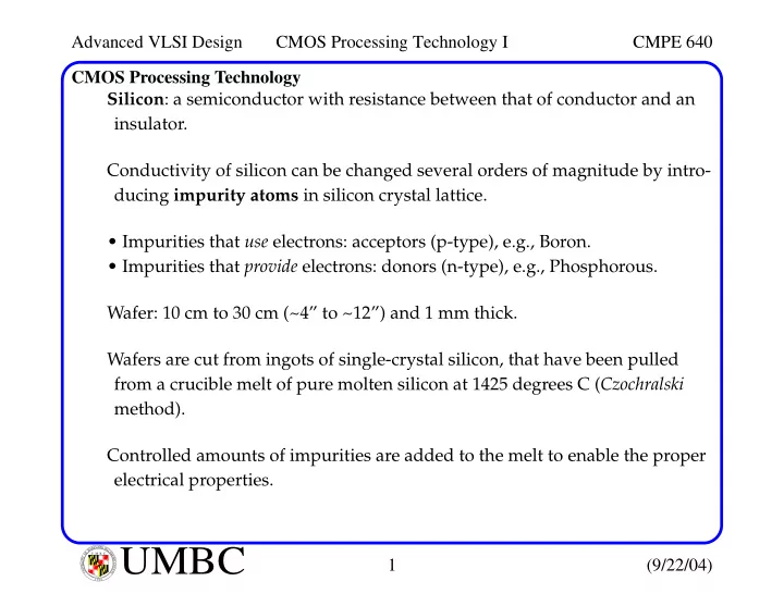
  1. Advanced VLSI Design CMOS Processing Technology I CMPE 640 CMOS Processing Technology Silicon : a semiconductor with resistance between that of conductor and an insulator. Conductivity of silicon can be changed several orders of magnitude by intro- ducing impurity atoms in silicon crystal lattice. • Impurities that use electrons: acceptors (p-type), e.g., Boron. • Impurities that provide electrons: donors (n-type), e.g., Phosphorous. Wafer: 10 cm to 30 cm (~4” to ~12”) and 1 mm thick. Wafers are cut from ingots of single-crystal silicon, that have been pulled from a crucible melt of pure molten silicon at 1425 degrees C ( Czochralski method). Controlled amounts of impurities are added to the melt to enable the proper electrical properties. L A N R Y D UMBC A B M A L T F O U M B C I M Y O R T 1 (9/22/04) I E S R C E O V U I N N U T Y 1 6 9 6
  2. Advanced VLSI Design CMOS Processing Technology I CMPE 640 Photolithography In each processing step, regions are selected for processing using photoli- thography and optical masks. Processing steps include: • Oxidation • Etching • Metal and polysilicon deposition • Ion implantation Optical mask Oxidation Photoresist Stepper coating exposure Photoresist Photoresist Repeat Photolithography steps development removal for each process step Spin, rinse, dry Acid etch Process Step L A N R Y D UMBC A B M A L T F O U M B C I M Y O R T 2 (9/22/04) I E S R C E O V U I N N U T Y 1 6 9 6

  3. Advanced VLSI Design CMOS Processing Technology I CMPE 640 Photolithography Process Oxidation layering Creates a layer of SiO 2 or glass for insulation. Wet Oxidation uses water vapor and Dry Oxidation uses high-purity oxygen and hydrogen at ~1000 degrees C. SiO 2 growth consumes silicon, grows into the substrate. SiO 2 is twice the volume of Si, projects above the substrate as well. Photoresist coating A light-sensitive polymer (latex) is evenly spread (thickness 1 µ m) by spinning the wafer. Negative photoresist : Unexposed photoresist soluble in organic solvent, light exposure causes cross-linking making exposed regions insoluble. Positive photoresist : Originally insoluble, exposure makes it soluble. Combining allows a single mask to be used for processing of comple- mentary regions in 2 processing steps. L A N R Y D UMBC A B M A L T F O U M B C I M Y O R T 3 (9/22/04) I E S R C E O V U I N N U T Y 1 6 9 6

  4. Advanced VLSI Design CMOS Processing Technology I CMPE 640 Photolithography Process Photoresist coating (continued) For example, to cut windows into the glass after oxidation step: Acid resistant coating (photoresist) spread evenly on surface. Photoresist SiO 2 (Glass) Silicon Wafer Stepper exposure A glass mask ( reticle , about 2 cm per side) containing the designer pat- terns is brought in close proximity to wafer. For negative photoresist , mask is opaque in regions to be processed. Ultraviolet (UV) light exposes transparent regions making photoresist insoluble. L A N R Y D UMBC A B M A L T F O U M B C I M Y O R T 4 (9/22/04) I E S R C E O V U I N N U T Y 1 6 9 6

  5. Advanced VLSI Design CMOS Processing Technology I CMPE 640 Photolithography Process Stepper exposure (continued) A stepper moves the reticle to successive locations on the wafer. Projection printing makes use of lenses between reticle and wafer to focus the pattern. Example: polymerized in areas exposed by UV light. UV light Mask Mask Photoresist SiO 2 Silicon Wafer L A N R Y D UMBC A B M A L T F O U M B C I M Y O R T 5 (9/22/04) I E S R C E O V U I N N U T Y 1 6 9 6

  6. Advanced VLSI Design CMOS Processing Technology I CMPE 640 Photolithography Process Photoresist development and bake Wafers developed in acid or base solution to remove exposed/unex- posed photoresist. Once removed, wafer is low temperature baked (soft baked) to harden remaining (unexposed/exposed) photoresist. Example: organic solvent removes polymerized areas. Photoresist SiO 2 Silicon Wafer L A N R Y D UMBC A B M A L T F O U M B C I M Y O R T 6 (9/22/04) I E S R C E O V U I N N U T Y 1 6 9 6

  7. Advanced VLSI Design CMOS Processing Technology I CMPE 640 Photolithography Process Acid etching Material is selectively removed from areas that are not covered by photo- resist using acids, bases and caustic solutions. Chemicals used here can be very dangerous to humans and the environ- ment. Hydrofluoric acid (HF) is used for SiO 2 . Example: windows are etched using HF. Photoresist SiO 2 Silicon Wafer L A N R Y D UMBC A B M A L T F O U M B C I M Y O R T 7 (9/22/04) I E S R C E O V U I N N U T Y 1 6 9 6

  8. Advanced VLSI Design CMOS Processing Technology I CMPE 640 Photolithography Process Spin, rinse and dry The wafer is cleaned with deionized water and dried with nitrogen. Cleaning reduces the chances of contamination. All processing is carried out in ultra-clean rooms (dust particles per cubic foot of air are maintained at 1 to 10). Processing step A processing step can now be applied to the wafer, including ion implantation, plasma etching or metal deposition. Photoresist removal (ashing) A high temperature plasma is used to remove the remaining photoresist. Example: photoresist removed. SiO 2 Silicon Wafer L A N R Y D UMBC A B M A L T F O U M B C I M Y O R T 8 (9/22/04) I E S R C E O V U I N N U T Y 1 6 9 6

  9. Advanced VLSI Design CMOS Processing Technology I CMPE 640 Photolithography Process Bear in mind that the example showed only one square that was etched. In reality, the entire chip is patterned and etched in parallel, possibly cre- ating hundreds of millions of such squares. Feature size reduction puts an enormous burden on semiconductor equip- ment manufacturers, particular those involved with optolithographically. The dimensions of features transcribed are smaller than the wavelengths of the optical light sources. Optical mask correction (OPC) warps the mask’s patterns to allow fea- ture sizes down to ~100 nm to overcome the diffraction phenomena. Phase shift masks (PSM) vary the thickness of the mask to create inter- ference patterns. These and other techniques increase resolution to 1/8 of the wavelength. Sources are lasers at 248 nm and 193 nm (future 157 nm and 13.4 nm) Extreme ultraviolet, X ray and electron beam are potential replacements. L A N R Y D UMBC A B M A L T F O U M B C I M Y O R T 9 (9/22/04) I E S R C E O V U I N N U T Y 1 6 9 6

  10. Advanced VLSI Design CMOS Processing Technology I CMPE 640 Diffusion and Ion Implantation Several steps in the manufacturing process require a change in the doping concentration of certain parts of the material. • Source and drain regions • Well and substrate contacts • Doping of the polysilicon • Adjustments to V t Several approaches exist, in the latter two, the regions to be doped are exposed and the rest of the wafer is coated with a buffer, typically SiO 2 . • Epitaxy : Single-crystal film grown on silicon surface with controlled impurities, that can have fewer defects than native wafer surface. • Diffusion implantation : Wafers are placed in quartz tube and heated to 900-1100 degrees C. The dopants are introduced via a gas and diffuse into the surface follow- ing a guassian profile. L A N R Y D UMBC A B M A L T F O U M B C I M Y O R T 10 (9/22/04) I E S R C E O V U I N N U T Y 1 6 9 6

  11. Advanced VLSI Design CMOS Processing Technology I CMPE 640 Diffusion and Ion Implantation • Ion implantation : The system sweeps a beam of purified dopants ions across the surface. Acceleration determines their depth of penetration while exposure time determines their concentration. Ion implantation more popular but requires a thermal annealing step to repair the silicon lattice. Deposition: Many of the layers of a CMOS process are introduced by deposition to act as either a buffer or as insulating or conducting layers. SiO 2 was given earlier as an example. Another is the use of silicon nitride, Si 3 N 4 , as a buffer for field oxide and stopper implant deposition. Chemical vapor deposition (CVD) is used to deposit Si 3 N 4 at tempera- tures of ~850 degrees C. L A N R Y D UMBC A B M A L T F O U M B C I M Y O R T 11 (9/22/04) I E S R C E O V U I N N U T Y 1 6 9 6

  12. Advanced VLSI Design CMOS Processing Technology I CMPE 640 Deposition and Etching Polysilicon is deposited using a CVD which flows silane gas (SiH 4 ) over a heated wafer coated with SiO 2 at ~650 degrees C. Deposition is followed by an implantation step to reduce poly resistance. Aluminum is deposited using sputtering , in which aluminum is evaporated using an electron-beam or ion-beam. It is then etched to form the wire interconnect (subtractive process). Copper is deposited selectively into trenches using a process called dual dam- ascene (additive process). Etching: Wet etching already discussed as a means to remove (etch) SiO 2 , typi- cally hydrofluoric acid + ammonium fluoride. L A N R Y D UMBC A B M A L T F O U M B C I M Y O R T 12 (9/22/04) I E S R C E O V U I N N U T Y 1 6 9 6

Download Presentation
Download Policy: The content available on the website is offered to you 'AS IS' for your personal information and use only. It cannot be commercialized, licensed, or distributed on other websites without prior consent from the author. To download a presentation, simply click this link. If you encounter any difficulties during the download process, it's possible that the publisher has removed the file from their server.

Recommend


More recommend