
SLIDE 1
Digital Systems Transmission Lines VIII CMPE 650 1 (4/8/08)
UMBC
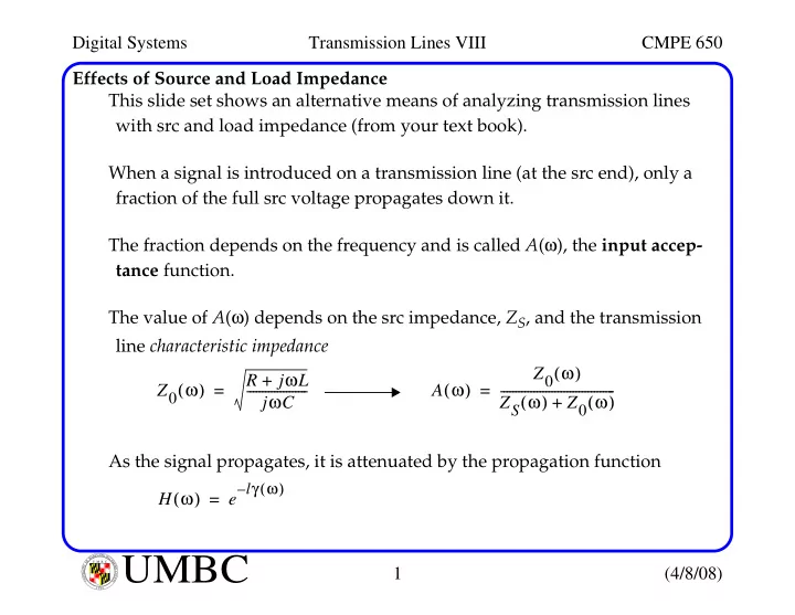
U M B C U N I V E R S I T Y O F M A R Y L A N D B A L T I M O R E C O U N T Y 1 9 6 6Effects of Source and Load Impedance This slide set shows an alternative means of analyzing transmission lines with src and load impedance (from your text book). When a signal is introduced on a transmission line (at the src end), only a fraction of the full src voltage propagates down it. The fraction depends on the frequency and is called A(ω), the input accep- tance function. The value of A(ω) depends on the src impedance, ZS, and the transmission line characteristic impedance As the signal propagates, it is attenuated by the propagation function Z0 ω ( ) R jωL + jωC
- =
A ω ( ) Z0 ω ( ) ZS ω ( ) Z0 ω ( ) +
- =
H ω ( ) e lγ ω
( ) –
=