
SLIDE 1
Advanced VLSI Design Details of the MOS Transistor I CMPE 640 1 (9/29/04)
UMBC
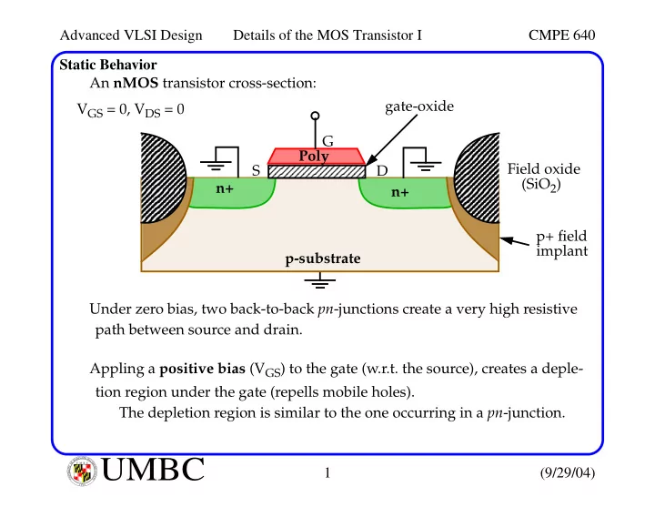
U M B C U N I V E R S I T Y O F M A R Y L A N D B A L T I M O R E C O U N T Y 1 9 6 6Static Behavior An nMOS transistor cross-section: Under zero bias, two back-to-back pn-junctions create a very high resistive path between source and drain. Appling a positive bias (VGS) to the gate (w.r.t. the source), creates a deple- tion region under the gate (repells mobile holes). The depletion region is similar to the one occurring in a pn-junction. G p-substrate Field oxide gate-oxide Poly n+ n+ (SiO2) p+ field implant S D VGS = 0, VDS = 0