
SLIDE 1
Advanced VLSI Design Combination Logic Design II CMPE 640 1 (11/17/04)
UMBC
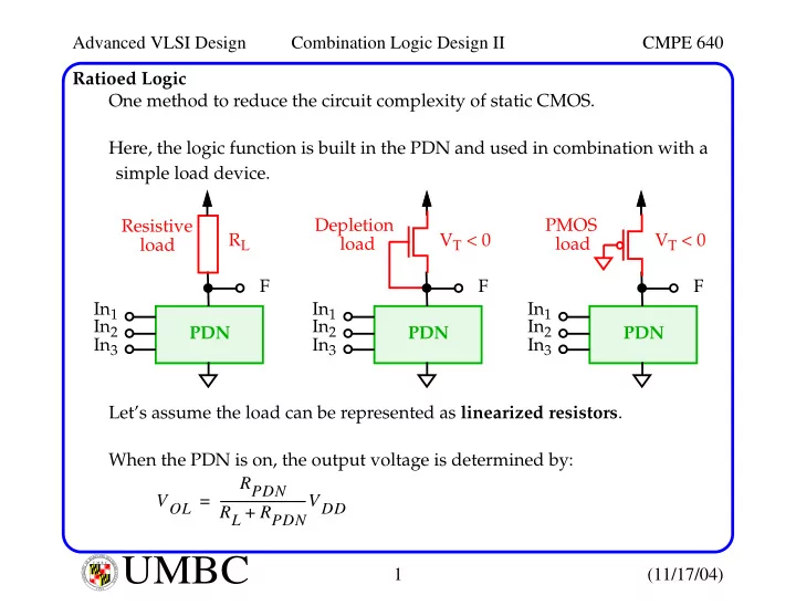
U M B C U N I V E R S I T Y O F M A R Y L A N D B A L T I M O R E C O U N T Y 1 9 6 6Ratioed Logic One method to reduce the circuit complexity of static CMOS. Here, the logic function is built in the PDN and used in combination with a simple load device. Let’s assume the load can be represented as linearized resistors. When the PDN is on, the output voltage is determined by: PDN In1 In2 In3 F RL Resistive load PDN In1 In2 In3 F VT < 0 Depletion load PDN In1 In2 In3 F VT < 0 PMOS load VOL RPDN RL RPDN +
- VDD
=