
SLIDE 1
VLSI Design Verification and Test Delay Faults II CMPE 646 1 (10/29/07)
UMBC
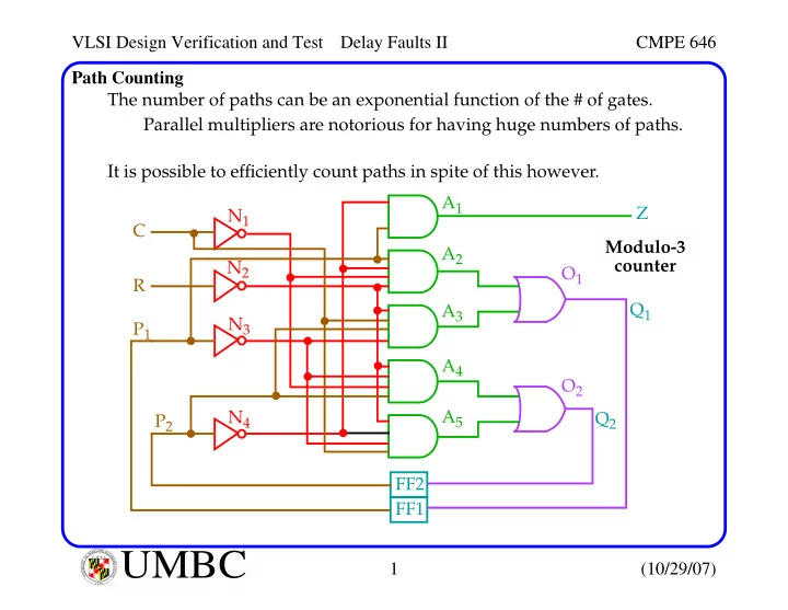
U M B C U N I V E R S I T Y O F M A R Y L A N D B A L T I M O R E C O U N T Y 1 9 6 6Path Counting The number of paths can be an exponential function of the # of gates. Parallel multipliers are notorious for having huge numbers of paths. It is possible to efficiently count paths in spite of this however. FF2 FF1 C N1 N2 N3 N4 A1 A2 A3 A4 A5 O1 O2 Z Q1 Q2 R Modulo-3 counter P1 P2