umbc
play

UMBC A B M A L T F O U M B C I M Y O R T 1 - PowerPoint PPT Presentation

VLSI Design Verification and Test Faults I CMPE 646 Defects, Errors and Faults Models bridge the gap between physical reality and a mathematical abstraction and allow for development of analytical tools. Definitions: Defect : An untended


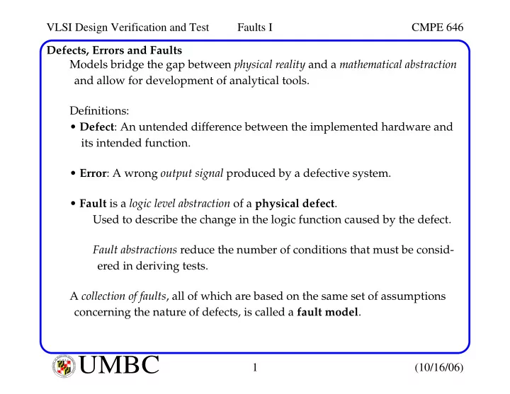
  1. VLSI Design Verification and Test Faults I CMPE 646 Defects, Errors and Faults Models bridge the gap between physical reality and a mathematical abstraction and allow for development of analytical tools. Definitions: • Defect : An untended difference between the implemented hardware and its intended function. • Error : A wrong output signal produced by a defective system. • Fault is a logic level abstraction of a physical defect . Used to describe the change in the logic function caused by the defect. Fault abstractions reduce the number of conditions that must be consid- ered in deriving tests. A collection of faults , all of which are based on the same set of assumptions concerning the nature of defects, is called a fault model . L A N R Y D UMBC A B M A L T F O U M B C I M Y O R T 1 (10/16/06) I E S R C E O V U I N N U T Y 1 6 9 6

  2. VLSI Design Verification and Test Faults I CMPE 646 Defects, Errors and Faults For example: A Out B A B Out A B Out 0 0 1 0 1 1 1 0 1 1 Ω 1 1 0 • Defect : A shorted to GND. • Fault : A Stuck-at logic 0. • Error : A = 1 , B = 1 => C = 1 Correct output is C = 0 . Note that the error is not permanent For example, no error occurs if at least one input is 0. L A N R Y D UMBC A B M A L T F O U M B C I M Y O R T 2 (10/16/06) I E S R C E O V U I N N U T Y 1 6 9 6

  3. VLSI Design Verification and Test Faults I CMPE 646 Functional Vs. Structural Testing For a 10-input AND gate, we can apply the test 0101010101 . 0 1 0 1 0 Out=0 1 0 1 0 1 If Out = 0 , what can we conclude? • (A) it’s an AND gate. • (B) it’s not a NAND gate. • (C) it’s a NOR gate. • (D) it’s not an OR gate. 2 2 10 There are Boolean functions possible. To be absolutely sure, we need to apply all 2 10 patterns. Clearly, functional test is not feasible. L A N R Y D UMBC A B M A L T F O U M B C I M Y O R T 3 (10/16/06) I E S R C E O V U I N N U T Y 1 6 9 6

  4. VLSI Design Verification and Test Faults I CMPE 646 Functional Vs. Structural Testing Design verification may need to use exhaustive functional tests. Fortunately, for hardware testing, we can assume the function is correct. The focus on structure makes it possible to develop algorithms that are independent of the design. The algorithms are based on fault models . Fault models can be formulated at the various levels of design abstraction. • Behavioral level : Faults may not have any obvious correlation to defects. • RTL and Logic level : Stuck-at faults most popular, followed by bridging and delay fault models. • Transistor (switch) level : Technology-dependent faults. I DDX : Defect-based methods Adv: can represent defects not represented by other fault models. L A N R Y D UMBC A B M A L T F O U M B C I M Y O R T 4 (10/16/06) I E S R C E O V U I N N U T Y 1 6 9 6

  5. VLSI Design Verification and Test Faults I CMPE 646 Design Levels from Testability Perspective : Behavioral Description Gate Behavioral DFT Technology Mapping Synthesis Layout Libraries RTL Description Parameter Extraction Libraries Logic DFT Synthesis Manufacturing Gate Description Product Test Pattern Generation (fault simulation) Test Application low high Fault Coverage? Good Product L A N R Y D UMBC A B M A L T F O U M B C I M Y O R T 5 (10/16/06) I E S R C E O V U I N N U T Y 1 6 9 6

  6. VLSI Design Verification and Test Faults I CMPE 646 Fault Models The text describes these and other fault models: • Bridging fault • Defect-oriented fault (e.g. bridging, stuck-open, I DDQ ). • Delay fault (transition, gate-delay, line-delay, segment-delay, path-delay). • Intermittent fault • Logical fault (often stuck-at) • Memory fault (single cell SA0/1, pattern sensitive, cell coupling faults). • Non-classical fault (stuck-open or stuck-on, transistor faults for CMOS). • Pattern sensitive fault • Pin fault (SA faults on the signal pins of all modules in the circuit). • Redundant fault • Stuck-at fault L A N R Y D UMBC A B M A L T F O U M B C I M Y O R T 6 (10/16/06) I E S R C E O V U I N N U T Y 1 6 9 6

  7. VLSI Design Verification and Test Faults I CMPE 646 Single stuck-at faults (SSF) Assumes defects cause the signal net or line to remain at a fixed voltage level. Model includes stuck-at-0 (SA0) or stuck-at-1 (SA1) faults and assumes only one fault exists. For example, how many SSF faults can occur on an n-input NAND gate? A B Inputs Fault-Free Faulty Response AB Response A/0 B/0 Z/0 A/1 B/1 Z/1 Z 00 1 1 1 0 1 1 1 01 1 1 1 0 0 1 1 10 1 1 1 0 1 0 1 11 0 1 1 0 0 0 1 What fault(s) does the pattern AB = 01 detect? What is the minimum number of tests needed to "detect" all of them? What are the tests? L A N R Y D UMBC A B M A L T F O U M B C I M Y O R T 7 (10/16/06) I E S R C E O V U I N N U T Y 1 6 9 6

  8. VLSI Design Verification and Test Faults I CMPE 646 SSF A dominant input value is defined as the value that determines the state of the output independent of the other values of the inputs. A B Inputs Fault-Free Faulty Response AB Response A/0 B/0 Z/0 A/1 B/1 Z/1 Z 00 1 1 1 0 1 1 1 01 1 1 1 0 0 1 1 10 1 1 1 0 1 0 1 11 0 1 1 0 0 0 1 What is the dominant input value for the NAND? How many tests do you need to diagnosis the fault? Can you distinguish between all of the faults? L A N R Y D UMBC A B M A L T F O U M B C I M Y O R T 8 (10/16/06) I E S R C E O V U I N N U T Y 1 6 9 6

  9. VLSI Design Verification and Test Faults I CMPE 646 SSF An n -line circuit can have at most 2n SSF faults. This number can be further reduced through fault collapsing . Fault detection requires: • A test t activates or provokes the fault f . • t propagates the error to observation point (primary output (PO)/scan latch). A line that changes with f is said to be sensitized to the fault site. Fault propagation requires off-path inputs be set to non-dominant values. 1 True response Faulty response AND1 1 1 0(1) AND2 0(1) 01 , 10 , and 11 0 do not provoke SA1 14 faults possible here. OR 0 the fault L A N R Y D UMBC A B M A L T F O U M B C I M Y O R T 9 (10/16/06) I E S R C E O V U I N N U T Y 1 6 9 6

  10. VLSI Design Verification and Test Faults I CMPE 646 SSF Let Z(t) represent the response of a circuit N under input vector t . Fault f transforms the circuit to N f and its response to Z f (t) . OR bridging defect Z 1 = x 1 x 2 Z 1f = x 1 + x 2 0(1) x 1 0(1) Z 2 = x 2 x 3 Z 2f = (x 1 + x 2 )x 3 Z 1 1 011 defects f because Z( 011 ) = 01 and x 2 Z f ( 011 ) = 11 . 1 Z 2 1 x 3 The set of all tests x that detect f is given by ( ) ⊕ ( ) Z x Z f x = 1 In this example, any test in which x 1 = 0 and x 4 = 1 is a test for f . x x 2 x 2 G 1 G 1 x 3 x x 3 Z f 0 G 3 x 1 G 3 0 x 1 Z = (x 2 + x 3 )x 1 + x 1 x 4 Z f = (x 2 + x 3 )x 1 G 5 1(0) 1(0) 1 G 2 ( ) ⊕ ( ) Z x Z f x x 1 x 4 = G 4 1 SA0 x 4 The expression x 1 x 4 represents 4 tests ( 0001 , 0011 , 0101 , 0111 ). L A N R Y D UMBC A B M A L T F O U M B C I M Y O R T 10 (10/16/06) I E S R C E O V U I N N U T Y 1 6 9 6

  11. VLSI Design Verification and Test Faults I CMPE 646 SSF Note that faults on fanout stems and fanout branches are not the same. Signal line g , h and i carry the same signal value. c h 0(1) j 1(0) 1 d SA0 a 1 z b g e k 0 i 1 f Input ab = ( 10 ) activates h SA0 and is detectable at z . This input also activates SA0 faults on g and i However, i SA0 is not detectable since it is blocked by f = 0. Stem g is the output of the NAND and lines h and i are inputs to downstream NANDs. To consider all possible faults, we model faults on all nodes g , h and i . L A N R Y D UMBC A B M A L T F O U M B C I M Y O R T 11 (10/16/06) I E S R C E O V U I N N U T Y 1 6 9 6

  12. VLSI Design Verification and Test Faults I CMPE 646 Fault Equivalence Two faults f and g are considered functionally equivalent iff Z f (x) = Z g (x). There is no test that can distinguish between f and g . i.e., all tests that detect f also detect g . For large circuits, determining this is computationally intensive. However, equivalence can be determined for simple gates and applied to large circuits. Any n -input gate has 2(n+1) SA faults. For the NAND gate, the SA0 on the inputs are equivalent to SA1 on the output and all three are detected by the same test pattern AB =( 11 ). For any n -input primitive gate with n >1, only n+2 single SA faults need to be considered. SA1 SA0 SA1 SA0 L A N R Y D UMBC A B M A L T F O U M B C I M Y O R T 12 (10/16/06) I E S R C E O V U I N N U T Y 1 6 9 6

  13. VLSI Design Verification and Test Faults I CMPE 646 Fault Equivalence Equivalence fault collapsing is performed from inputs to output. A H B Z 10/20 = 0.5 remain C F G V D {A/0, B/0, H/0} E {C/1, D/1, F/1, G/0} merge {E/0, G/0, V/0} {H/1, V/1, Z/1} {F/0, G/1} 20/32 = 0.625 remain Reduction is between 50-60% and is larger, in general, for fanout free circuits. L A N R Y D UMBC A B M A L T F O U M B C I M Y O R T 13 (10/16/06) I E S R C E O V U I N N U T Y 1 6 9 6

Download Presentation
Download Policy: The content available on the website is offered to you 'AS IS' for your personal information and use only. It cannot be commercialized, licensed, or distributed on other websites without prior consent from the author. To download a presentation, simply click this link. If you encounter any difficulties during the download process, it's possible that the publisher has removed the file from their server.

Recommend


More recommend