
SLIDE 1
VLSI Design Verification and Test Fault Simulation I CMSC 691x 1 (Oct 18, 2001)
UMBC
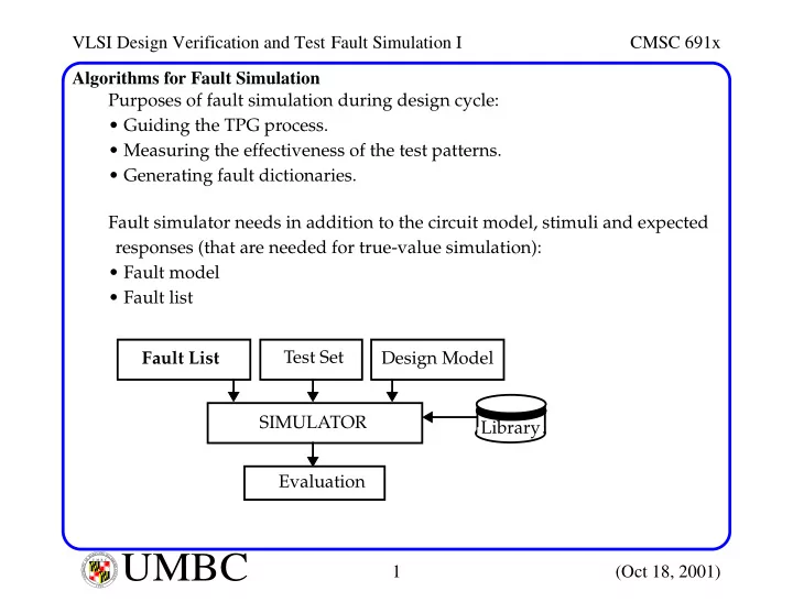
U M B C U N I V E R S I T Y O F M A R Y L A N D B A L T I M O R E C O U N T Y 1 9 6 6Algorithms for Fault Simulation Purposes of fault simulation during design cycle:
- Guiding the TPG process.
- Measuring the effectiveness of the test patterns.
- Generating fault dictionaries.
Fault simulator needs in addition to the circuit model, stimuli and expected responses (that are needed for true-value simulation):
- Fault model
- Fault list
Test Set Design Model SIMULATOR Library Evaluation Fault List