
SLIDE 1
Advanced VLSI Design Memory CMPE 640 1 (12/8/04)
UMBC
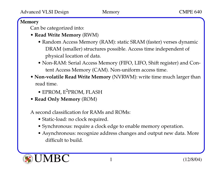
U M B C U N I V E R S I T Y O F M A R Y L A N D B A L T I M O R E C O U N T Y 1 9 6 6Memory Can be categorized into:
- Read Write Memory (RWM)
- Random Access Memory (RAM): static SRAM (faster) verses dynamic
DRAM (smaller) structures possible. Access time independent of physical location of data.
- Non-RAM: Serial Access Memory (FIFO, LIFO, Shift register) and Con-
tent Access Memory (CAM). Non-uniform access time.
- Non-volatile Read Write Memory (NVRWM): write time much larger than
read time.
- EPROM, E2PROM, FLASH
- Read Only Memory (ROM)
A second classification for RAMs and ROMs:
- Static-load: no clock required.
- Synchronous: require a clock edge to enable memory operation.
- Asynchronous: recognize address changes and output new data. More
difficult to build.