
SLIDE 1
Advanced VLSI Design Combination Logic Design IV CMSC 613 1 (Nov. 19, 2001)
UMBC
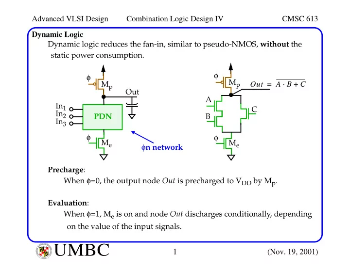
U M B C U N I V E R S I T Y O F M A R Y L A N D B A L T I M O R E C O U N T Y 1 9 6 6Dynamic Logic Dynamic logic reduces the fan-in, similar to pseudo-NMOS, without the static power consumption. Precharge: When φ=0, the output node Out is precharged to VDD by Mp. Evaluation: When φ=1, Me is on and node Out discharges conditionally, depending
- n the value of the input signals.
PDN In1 In2 In3 Out φ φ Me Mp φn network φ φ Me Mp A B C Out A B ⋅ C + =