TRIPS: A Distributed Explicit Data Graph Execution (EDGE) - PDF document
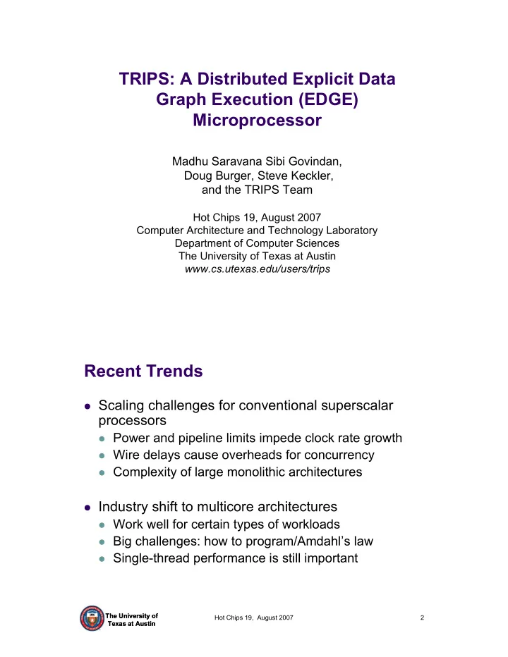
TRIPS: A Distributed Explicit Data Graph Execution (EDGE) Microprocessor Madhu Saravana Sibi Govindan, Doug Burger, Steve Keckler, and the TRIPS Team Hot Chips 19, August 2007 Computer Architecture and Technology Laboratory Department of
TRIPS: A Distributed Explicit Data Graph Execution (EDGE) Microprocessor Madhu Saravana Sibi Govindan, Doug Burger, Steve Keckler, and the TRIPS Team Hot Chips 19, August 2007 Computer Architecture and Technology Laboratory Department of Computer Sciences The University of Texas at Austin www.cs.utexas.edu/users/trips Recent Trends � Scaling challenges for conventional superscalar processors � Power and pipeline limits impede clock rate growth � Wire delays cause overheads for concurrency � Complexity of large monolithic architectures � Industry shift to multicore architectures � Work well for certain types of workloads � Big challenges: how to program/Amdahl’s law � Single-thread performance is still important The University of The University of Hot Chips 19, August 2007 2 Texas at Austin Texas at Austin
TRIPS – A Technology Scalable Architecture Goals � High single-thread performance through ILP � Exploit concurrency at multiple granularities � Scalable with technology trends � Key technologies � Explicit data graph execution (EDGE) ISA � Distributed processor microarchitecture � Distributed non-uniform (NUCA) L2 cache � Tiled and networked design � Hot Chips 2005 - Chip in RTL design phase � Hot Chips 2007 - Chip/system complete � Manufacturing/bring-up complete � Performance tuning in progress � This talk focuses on chip and system � implementation The University of The University of Hot Chips 19, August 2007 3 Texas at Austin Texas at Austin Outline � Explicit Data Graph Execution (EDGE) ISAs � ISA support for distributed execution � TRIPS networked microarchitecture � Processor microarchitecture � Non-uniform cache memory system � TRIPS chip and system implementation � Custom ASIC chip and system boards � Preliminary performance results The University of The University of Hot Chips 19, August 2007 4 Texas at Austin Texas at Austin
Explicit Data Graph Execution (EDGE) � Two key features Program broken into sequence of instruction blocks � � Execution model: fetch, execute, and commit blocks atomically � Amortize overheads over many instructions Within a block, instructions explicitly encode producer-consumer � communication � Producer instructions explicitly targets consumers and send results directly to them (without using a register file) � Instructions “fire” when all operands arrive � Any instruction may be predicated (conditionally executed) � TRIPS blocks - up to 128 instructions Compile-time techniques to create large blocks � Average block sizes typically greater than 45 instructions � Long-term goal: hide hard-to-predict branches inside blocks � The University of The University of Hot Chips 19, August 2007 5 Texas at Austin Texas at Austin TRIPS Execution Model if (p==0) Program if-then-else Control Flow example z = a * 2 + 3; Graph (CFG) else z = b * 3 + 4; Basic Block TRIPS block p a b TRIPS block for if-then-else teqz muli muli TRIPS block addi addi st(1) CFG Loop Example if-then-else Example The University of The University of Hot Chips 19, August 2007 6 Texas at Austin Texas at Austin
TRIPS Execution Model Time (cycles) 0 5 10 30 40 B i Block 8 Block 0 B i+8 FETCH EXECUTE COMMIT (variable execution time) Structural Block 1 B i+1 dependence Block 2 B i+2 In-flight blocks/instructions Block 3 B i+3 Block 4 B i+4 Block 5 B i+5 Block 6 B i+6 Block 7 B i+7 Fetch/Execute/Commit overlapped across multiple blocks � Can execute up to 8 blocks at a time via speculation � Exposes concurrency with a very large instruction window � Single-threaded mode with up to 1024 instructions � Simultaneous multi-threaded (SMT) mode with up to 4 threads and � 256 instruction window per thread The University of The University of Hot Chips 19, August 2007 7 Texas at Austin Texas at Austin TRIPS Prototype Chip EBI IRQ (External Bus (Interrupt Interface) Request) 2 TRIPS Processors DDR � GPIO JTAG CLK 44 SDRAM NUCA L2 Cache � 108 16 1 MB, 16 banks � On-Chip Network (OCN) � DMA SDC EBC TEST PLLS 2D mesh network � Replaces on-chip bus � OCN Controllers � 2 DDR SDRAM controllers � PROC 0 2 DMA controllers � External Bus Controller (EBC) � NUCA Interfaces with PowerPC 440GP � (control processor) L2 Chip-to-Chip (C2C) network controller � Cache Clocking � PROC 1 2 PLLs � 4 Clock domains � 1x and 2x SDRAM � Main and C2C � Clock tree DMA SDC C2C � Main domain has 4 quadrants to � limit local skew 108 8x39 DDR C2C SDRAM Links The University of The University of Hot Chips 19, August 2007 8 Texas at Austin Texas at Austin
TRIPS Microarchitecture Principles � Distributed and tiled architecture Small and simple tiles (register file, data cache bank, etc.) � Short local wires � � Tiles are small: 2-5 mm 2 per tile is typical No centralized resources � � Networks connect the tiles Networks implement distributed protocols (I-fetch, bypass, etc.) � � Includes well-defined control and data networks Networks connect only nearest neighbors � No global wires � � Design modularity and scalability Design productivity by replicating tiles (design reuse) � Networks extensible, even late in design cycle � The University of The University of Hot Chips 19, August 2007 9 Texas at Austin Texas at Austin TRIPS Tile-level Microarchitecture TRIPS Tiles G:Processor control - TLB w/ variable size pages, dispatch, next block predict, commit R: Register file - 32 registers x 4 threads, register forwarding I: Instruction cache - 16KB storage per tile D: Data cache - 8KB per tile, 256-entry load/store queue, TLB E: Execution unit - Int/FP ALUs, 64 reservation stations M: Memory - 64KB, configurable as L2 cache or scratchpad N: OCN network interface - router, translation tables DMA: Direct memory access controller SDC: DDR SDRAM controller EBC: External bus controller - interface to external PowerPC C2C: Chip-to-chip network controller - 4 links to XY neighbors The University of The University of Hot Chips 19, August 2007 10 Texas at Austin Texas at Austin
TRIPS Processor � EDGE ISA blocks mapped to array of tiles Compile-time scheduler decides where (not when) instructions � execute � TRIPS: aggressive processor capabilities Up to 16 instructions per cycle � Up to 4 loads/stores per cycle � Up to 64 outstanding L1 data cache misses � Up to 1024 dynamically scheduled instructions � Up to 4 simultaneous multithreading (SMT) threads � � Memory system 4 simultaneous L1 cache fills per processor � Up to 16 simultaneous L2 cache accesses � Up to 16 outstanding L2 cache misses � The University of The University of Hot Chips 19, August 2007 11 Texas at Austin Texas at Austin Non-Uniform (NUCA) L2 Cache 1MB L2 cache � Sixteen tiled 64KB banks Bank Bank � On-chip network PROC 0 � Bank Bank 4x10 2D mesh topology � 128-bit links, 366MHz (4.7GB/sec) Bank Bank � 4 virtual channels prevent deadlocks � Bank Bank Requests and replies are wormhole- � routed across the network Bank Bank Up to 10 memory requests per cycle � Request Up to 128 bytes per cycle returned to Bank Bank � Reply PROC 1 the processors Bank Bank Individual banks reconfigurable as � scratchpad Bank Bank The University of The University of Hot Chips 19, August 2007 12 Texas at Austin Texas at Austin
TRIPS Project Timeline 1999 2000 2001 2002 2003 2004 2005 2006 2007 Technology trend analysis “What are the problems to solve?” New architecture concepts, invention, publishing “What are the solutions?” Prototype design “Solve detailed challenges of architecture.” UT-Austin team � Prototype implementation 12 graduate students + 1 � “Is it feasible?” engineer RTL, verification, timing � Prototype testing. IBM ASIC team � “Does it work; how well?” Physical design � Unveiling The University of The University of Hot Chips 19, August 2007 13 Texas at Austin Texas at Austin TRIPS Chip Implementation 130nm ASIC with 7 metal Process Technology layers 18.3mm x 18.37mm Die Size (336 mm 2 ) Package 47mm x 47mm BGA 626 signals, 352 Vdd, 348 Pin Count GND # of placed cells 6.1 million Transistor count (est.) 170 million # of routed nets 6.5 million Total wire length 1.06 km 36W at 366MHz Power (measured) (chip has no power mgt.) 2.7ns (actual) Clock period 4.5ns (worse case sim) The University of The University of Hot Chips 19, August 2007 14 Texas at Austin Texas at Austin
Die Photos With C4 Array Without C4 Array The University of The University of Hot Chips 19, August 2007 15 Texas at Austin Texas at Austin Benefits of Tiled Design � Design modularity � 11 different tiles, instantiated a total of 106 times � Clean interfaces at tile boundaries � Verification - no hardware bugs � Tiles verified extensively before stitching together � Place and Route - hierarchical in nature � Wiring only between nearest neighbors � But - each physical instance was a little different � Timing - trivial at top level, communication planned � No global wires or timing paths The University of The University of Hot Chips 19, August 2007 16 Texas at Austin Texas at Austin
Recommend
More recommend
Explore More Topics
Stay informed with curated content and fresh updates.


