
SLIDE 1
Contents Theory & Design Fabrication Packaging
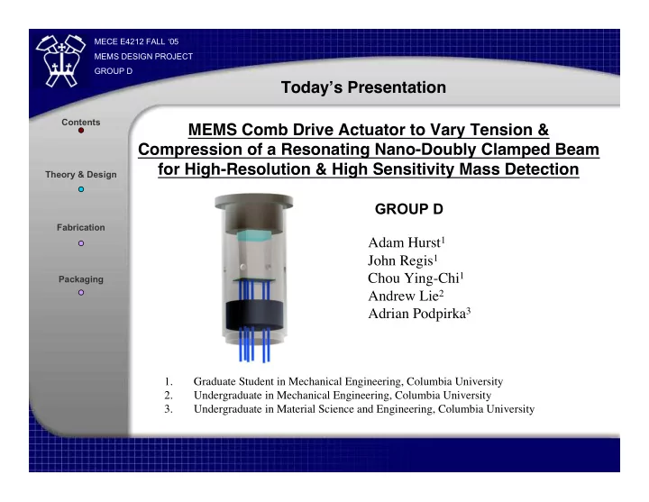
MEMS Comb Drive Actuator to Vary Tension & Compression of a Resonating Nano-Doubly Clamped Beam for High-Resolution & High Sensitivity Mass Detection
MECE E4212 FALL ‘05 MEMS DESIGN PROJECT GROUP D