
SLIDE 1
The Next Generation of Cryptanalytic Hardware FPGAs (Field - - PowerPoint PPT Presentation
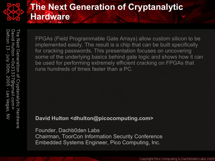
The Next Generation of Cryptanalytic Hardware FPGAs (Field Programmable Gate Arrays) allow custom silicon to be implemented easily. The result is a chip that can be built specifically for cracking passwords. This presentation focuses on
Educational purposes only Full disclosure I'm not a hardware guy
Introduction to FPGAs
What is an FPGA? Gate Logic
Cracking \w Hardware
History
Optimizations
Pipelines Parallelism
Chipper
Lanman/NTLM Demo Performance
Field Programmable Gate Array
Lets you prototype IC's Code translates directly into circuit logic
The basic building blocks of any computing
Build other types of logic, such as adders:
Which can be chained together:
And can be used for storing values:
Feedback Flip-Flop /
JK Flip-Flop
This can be implemented with electronics:
NOT AND
An FPGA is an array of configurable gates
Gates can be connected together arbitrarily States can be configured Common components are provided Any type of logic can be created
Configurable Logic Blocks (CLBs)
Registers (flip flops) for fast data storage Logic Routing
Input/Output Blocks (IOBs)
Basic pin logic (flip flops, muxs, etc)
Block Ram
Internal memory for data storage
Digial Clock Managers (DCMs)
Clock distribution
Programmable Routing Matrix
Intelligently connects all components together
PPC
Pros
Common Hardware Benefits
Massively parallel Pipelineable
Reprogrammable
Self-reconfiguration
Cons
Size constraints / limitations More difficult to code & debug
Common Applications
Encryption / decryption AI / Neural networks Digital signal processing (DSP) Software radio Image processing Communications protocol decoding Matlab / Simulink code acceleration Etc.
Common Applications
Encryption / decryption AI / Neural networks Digital signal processing (DSP) Software radio Image processing Communications protocol decoding Matlab / Simulink code acceleration Etc.
Antifuse
Programmable only once
Flash
Programmable many times
SRAM
Programmable dynamically Most common technology Requires a loader (doesn't keep state after power-
Xilinx
Virtex-4 Optional PowerPC Processor
Altera
Stratix-II
Hardware Description Language Simple C-like Syntax Like Go - Easy to learn, difficult to master
One bit AND
C Verilog Gate
8 bit AND
C Verilog Gate
8 bit Flip-Flop
C Verilog Gate
Minimal Key Lengths for Symmetric Ciphers
Ronald L. Rivest (R in RSA) Bruce Schneier (Blowfish, Twofish, etc) Tsutomu Shimomura (Mitnick) A bunch of other ad hoc cypherpunks
40-bit SSL is crackable by almost anyone 56-bit DES is crackable by companies Scared yet?
1998
The Electronic Frontier Foundation (EFF) Cracked DES in < 3 days Searched ~9,000,000,000 keys/second Cost < $250,000
2001
Richard Clayton & Mike Bond (University of
Cracked DES on IBM ATMs Able to export all the DES and 3DES keys in ~ 20
Cost < $1,000 using an FPGA evaluation board
2002
Rouvroy Gael, Standaert Francois-Xavier and others
Implemented a linear cryptanalysis attack on DES Used FPGAs to generate dictionary tables Chosen-plaintext attack can recover key in 10 seconds
2004
Philip Leong, Chinese University of Hong Kong IDEA
50Mb/sec on a P4 vs. 5,247Mb/sec on Pilchard
RC4
Cracked RC4 keys 58x faster than a P4 Parallelized 96 times on a FPGA Cracks 40-bit keys in 50 hours Cost < $1,000 using a RAM FPGA (Pilchard)
PC
Hardware
PC
Speed scales with # of instructions & clock speed
Hardware
Speed scales with FPGA's:
Size Clock Speed
PC
Hardware
PC
Hardware
PC
Hardware
PC
Hardware
PC
Hardware
PC
Speed scales with # of instructions & clock speed
Hardware
Speed scales with FPGA's:
Size Clock speed Slowest operation in the pipeline
PC
PC
PC
DSP48
Configurable 18x18-bit Multiplier 48+48-bit Adder Input/Output Registers 18x18 Multiplies @ 500MHz Virtex-4 LX25 comes with 48
BlockRAM
Stores up to 18Kb From 1 to 36 bits Dual-port FIFO Support Virtex-4 LX25 comes with 72
Auxiliary Processing Unit (APU)
PowerPC allows you to implement custom instructions Have access to all of the registers Single instruction from processor triggers your logic e.g. Single instruction DES
Currently Supports
Unix DES Windows Lanman Windows NTLM (full-support coming soon) Multiple Cards/FPGAs ;-)
Lanman
14-Character Passwords Case insensitive (converted to upper case) Split into 2 7-byte keys Used as key to encrypt static values with DES
Hardware Design
Pipeline design Internal cracking engine passwords = lmcrack(hashes, options); Interface over PCMCIA Can specify cracking options
Bits to search e.g. Search 55-bits (instead of 56) Offset to start search e.g. First card gets offset 0, second card gets offset 2**55 Typeable/printable characters Alpha-numeric Allows for basic distributed cracking & resume functionality
Software Design – Thanks Arachne!!
GUI and Console Interfaces WxWidgets
Windows Linux MacOS X (coming soon)
Supports cracking 128 keys in parallel on each
Supports 4x fast mode for just one hash pair Can automatically load required FPGA image Supports multiple card clusters
PC
~ 2,000,000 c/s
Hardware
125Mhz = 125,000,000 c/s per core 500Mhz = 500,000,000 c/s for fast mode!
Pico E-12
Compact Flash Type-II Form Factor Virtex-4 (LX25 or FX12)
1 Million Gates (~25,000 CLBs) Optional 450 MHz PowerPC Processor
128 MB PC-133 RAM 64 MB Flash ROM Gigabit Ethernet JTAG Debugging Port
Sourceforge project
Chipper Lanman & NTLM cracking cores Modular Exponentiation A5/2 (for some GSM research)
Technology Trends
Embedded platforms are either cheap and slow or
There will always be a cost factor with regards to
This has plagued smart cards, speedpasses,
The future is definitely implementing more
As cheap chips get faster, the workload for brute-
Elegance will be the next generation
FPGAs are increasing according to Moore's Law
Different factors though
Density - Increasing Clock Speed - Increasing Components – Created and expanded to fit markets Cost - Dropping
Slowly starting to compete with ASICs Future Applications:
Neural Networks Attacks on WEP/WPA/GSM Analysis and Correlation
What do you think? Possible Applications? Questions?
David Hulton
h1kari@dachb0den.com
OpenCiphers
http://www.openciphers.org
OpenCores
http://www.opencores.org
Xilinx
ISE Foundation (Free 60-day trial)
Pico Computing, Inc.
http://www.picocomputing.com