The Logic Circuit CAD Process Introduction This series of lectures - - PDF document

the logic circuit cad process introduction
SMART_READER_LITE
LIVE PREVIEW

The Logic Circuit CAD Process Introduction This series of lectures - - PDF document

Robert Betz: 97 Department of Electrical and Computer Engineering The Logic Circuit CAD Process Introduction This series of lectures looks at the CAD process using the tool set supplied by Altera. This tool set has its own particular way of


slide-1
SLIDE 1

Department of Electrical and Computer Engineering

Slide 1

Robert Betz: 97

The Logic Circuit CAD Process Introduction

This series of lectures looks at the CAD process using the tool set supplied by Altera. This tool set has its own particular way of implementing the design process, but is representative of tool sets by other vendors.
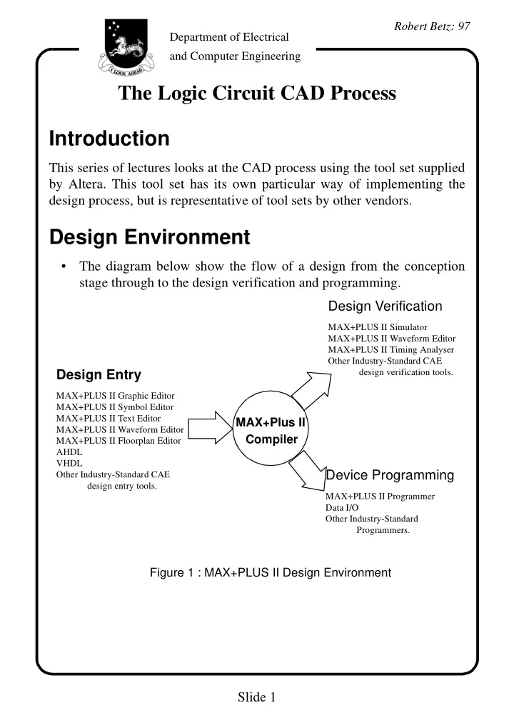
Design Environment

  • The diagram below show the flow of a design from the conception

stage through to the design verification and programming.

MAX+Plus II Compiler

Design Entry

MAX+PLUS II Graphic Editor MAX+PLUS II Symbol Editor MAX+PLUS II Text Editor MAX+PLUS II Waveform Editor MAX+PLUS II Floorplan Editor AHDL VHDL Other Industry-Standard CAE design entry tools.

Design Verification

MAX+PLUS II Simulator MAX+PLUS II Waveform Editor MAX+PLUS II Timing Analyser Other Industry-Standard CAE design verification tools.

Device Programming

MAX+PLUS II Programmer Data I/O Other Industry-Standard Programmers.

Figure 1 : MAX+PLUS II Design Environment

slide-2
SLIDE 2

Department of Electrical and Computer Engineering

Slide 2

Robert Betz: 97

Design Flow

  • 1. Create a new design file or a hierarchy of multiple design files in any

combination of the MAX+PLUS II design editors, i.e. Graphic, Text

  • r Waveform editors.
  • 2. Specify the top-level design file name as the project name.
  • 3. Assign a device family for the project. You can either allow the Com-

piler to select a device for you or assign a specific device.

  • 4. Open MAX+PLUS II compiler window and choose the Start button

to compile the project. You can turn on the SNF extractor module to create a netlist file for timing simulation and timing analysis.

  • 5. If project compiles successfully, you can optionally perform a simula-

tion and timing analysis: (i) To run a timing analysis, open the MAX+PLUS II Timing Ana- lyser window, select an analysis mode, and choose the Start but- ton. (ii) To run a simulation, you must first create vector inputs in a Simu- lator Channel File (.scf) in the Waveform Editor or in a Vector File (.vec) in the Text Editor. Then open the MAX+PLUS II Sim- ulator window and choose the Start button.

  • 6. Open the MAX+PLUS II Programmer window and either insert a

device into a programmer adapter on the Master Programming Unit (MPU) or connect the BitBlaster to a device that is mounted in-sys- tem.

  • 7. Choose the Program button to program an EPROM, EEPROM or

FLASH-based device, or choose the Configure button to configure an SRAM-based device.

slide-3
SLIDE 3

Department of Electrical and Computer Engineering

Slide 3

Robert Betz: 97

Files in the Environment

  • Three main sets of files in the design environment:

Design Files

A design file is either a graphic, text or waveform file created with the MAX+PLUS II Graphic, Text or Waveform Editor, or with another industry standard schematic or text editor or an EDIF or VHDL netlist writer. Design files are processed by the compiler. The compiler can compile the following file types:

  • Graphic Design Files (.gdf).
  • Text Design Files (.tdf).
  • Waveform Design Files (.wdf).
  • VHDL Design Files (.vhd).
  • OrCAD Schematic Files (.sch).
  • EDIF Input Files (.edf)
  • Xilinx Netlist Format Files (.xnf).
  • Altera Design Files (.adf).
  • State Machine Files (.smf)

Ancillary Files

These are files that are associated with the MAX+PLUS II project but are not part of the project tree hierarchy. Most files of this type do not con- tain design logic. some are automatically generated by the design envi- ronment, others are user entered, e.g. Assignment and configuration files (.acf), Symbol files (.sym), report files (.rpt), vector files (.vec).

slide-4
SLIDE 4

Department of Electrical and Computer Engineering

Slide 4

Robert Betz: 97

Projects

  • A project consists of all the files in a design hierarchy, including the

ancillary files and the output files.

  • Project name is the name of the top-level design file, without the

file name extension. The user nominates the project file.

  • Each project should be placed in a separate directory of the

\max2plus directory.

slide-5
SLIDE 5

Department of Electrical and Computer Engineering

Slide 5

Robert Betz: 97

Design Tools

Design Entry

Max+PLUS II Graphic Editor Max+PLUS II Text Editor Max+PLUS II Waveform Editor Max+PLUS II Symbol Editor Max+PLUS II Floorplan Editor Top- Level File Top-level design files can be .gdf, .sch, .tdf, .vhd or .edf .gdf .sch .wdf .tdf .vhd .edf .xnf .adf .smf .gdf Graphic file Graphic file Waveform file Text file Text file Text file Text file Text file Text file Imported from industry-standard CAE tools Imported from A+PLUS or SAM+PLUS to the MAX+PLUS II Compiler

Figure 2 : MAX+PLUS II Design Entry Methods

slide-6
SLIDE 6

Department of Electrical and Computer Engineering

Slide 6

Robert Betz: 97

MAX+PLUS II Graphic Editor

  • Offers WYSIWYG graphic design environment.
  • Allows schematic capture of a design.
  • Supports primitive, megafunction and macrofunction libraries,

including the Library of Parameterized Modules (LPM).

  • Has a symbol generation capability to make building hierarchical

designs simple.

  • A Graphic Design File (.gdf) can include any combination of prim-

itive and macrofunction symbols. Symbols can represent any type

  • f design file.

Figure 3 : Graphic Editor screen in the MAX+PLUS II Development Environment.

slide-7
SLIDE 7

Department of Electrical and Computer Engineering

Slide 7

Robert Betz: 97

MAX+PLUS II Symbol Editor

  • Enables one to view, create, and edit a symbol that represents a

logic circuit.

  • Symbol files have the same name as the design file it represents,

with the extension .sym. The Create Default Symbol command, available from the File menu of the Graphic, Text and Waveform Editors, creates a symbol from any design file.

MAX+PLUS II Text Editor

  • A tool for entering Text Design Files in Altera Hardware Descrip-

tion Language (AHDL) (.tdf) or Very High Speed Integrated Cir- cuit Hardware Description Language (VHDL) (.vhd).

Figure 4 : Symbol Editor screen in the MAX+PLUS II Development Environment.

slide-8
SLIDE 8

Department of Electrical and Computer Engineering

Slide 8

Robert Betz: 97

  • Can also edit any ascii file as well.
  • Offers feature that support the Altera design environment -e.g. syn-

tax highlighting, automatic location of compilation errors, tem- plates for AHDL and VHDL.

  • Offers a link to the compiler or simulation.

MAX+PLUS II Waveform Editor

  • Serves two roles: a design entry tool, and as a tool for entering test

vectors and viewing simulation results.

  • Waveform Design Files (.wdf) can contain design logic for a spe-

cific project. These files offer an alternative to graphic or text entry for a design. One creates a design by specifying the input wave- forms and the output waveforms. One can also generate state

Figure 5 : Text Editor screen in the MAX+PLUS II Development Environment

slide-9
SLIDE 9

Department of Electrical and Computer Engineering

Slide 9

Robert Betz: 97

machines as well using this method.

  • One can also create Simulator Channel Files (.scf) that contain

input vectors for simulation and functional testing.

Floorplan Editor

  • Allows physical resources to be assigned and to view Compiler par-

titioning and fitting results.

  • Has two displays:

(a) The device view shows all pins on the device package and their function. (b) The LAB view shows the interior of the device, including all Logic Array Blocks (LABs) and the individual logic cells within each LAB.

Figure 6 : Waveform Editor screen in the MAX+PLUS II Development Environment

slide-10
SLIDE 10

Department of Electrical and Computer Engineering

Slide 10

Robert Betz: 97

  • Provides a list of unassigned node and pin names in your project,

the handles to which can be dragged to an individual pin, logic cell, I/O cell, or embedded cell in the Device View or LAB view display. One can also drag and assigned pin or node to the list of unassigned nodes.

Altera Hardware Description Language (AHDL)

  • High level modular language that is completely integrated into the

MAX+PLUS system.

  • AHDL files can be created with a normal text editor or with the edi-

tor included in the MAX+PLUS II system. This has some advan- tages because of the tight connect of AHDL into the Altera development system.

Figure 7 : Floorplan Editor screen in the MAX+PLUS II Development Environment

slide-11
SLIDE 11

Department of Electrical and Computer Engineering

Slide 11

Robert Betz: 97

  • AHDL consists of a variety of elements and behavioural statements

that describe logic.

  • AHDL is an ideal tool for describing functions such as state

machines, truth tables, boolean equations, conditional logic, and group operations.

  • One can use Library Parameterized Modules (LPM) functions to

implement logic. LPMs provide gate, arithmetic, and storage com- ponents that implement combinational logic such as decoders, mul- tiplexers, and adders, and sequential logic such as registers and counters.

  • AHDL is ideal for state machine designs: one can assign state bits

and state values, or let the compiler do the work for you. See Figure 8 overleaf

VHDL

  • Very High Speed Integrated Circuit (VHSIC) Hardware Description

Language is a high level, modular language that is completely inte- grated into the MAX+PLUS II system.

  • VHDL is an industry standard hardware description language that

describes inputs and outputs, behaviour, and function of circuits. Defined by IEEE Standard 1076-1987.

  • VHDL files (.vhd) created by a standard text editor or by the inte-

grated text editor.

Primitives, Megafunctions & Macrofunctions

  • Altera provides libraries of logic functions – primitives, megafunc-

tions, and old style (e.g. 74 series TTL) macrofunctions, including functions that are optimized for the architecture of a particular device family.

  • All logic functions are copied to subdirectories of \maxplus2\max-

lib and \maxplus2\max2vhdl directories.

slide-12
SLIDE 12

Department of Electrical and Computer Engineering

Slide 12

Robert Betz: 97

Primitives

  • Examples: buffer, flip-flop, latch, input/output, and logic primi-

tives.

  • These are the basic functional blocks used to design circuits.
  • If a primitive is connected to a named bus then the compiler will

Figure 8 : Part of an AHDL program

slide-13
SLIDE 13

Department of Electrical and Computer Engineering

Slide 13

Robert Betz: 97

automatically expand the number of primitives to the number of bus lines saving space and design entry time.

Megafunctions

  • Complex or high level building blocks that can be used together

with primitives and other mega and macrofunctions to create a logic design.

  • LPMs are an example of a megafunction that is parameterized – i.e.

the user can set the size, behaviour and silicon implementation.

  • Megafunctions can be used freely in GDFs and TDFs; non-parame-

terized megafunctions can be used in VHDL design files.

  • The compiler automatically removes any unused gates and flip-

flops to ensure optimum design efficiency.

Old Style Macrofunctions

  • Similar to megafunctions above
  • Not inherently parameterized.
  • Altera recommends using LPMs instead – scalable and use the sili-

con more efficiently.

Project Hierarchy

  • Allows the display of the design hierarchy where the lower level

files are represented as branches.

  • This display makes it easy to move between the different files that

make up a design. Also shows the relationship between all the dif- ferent sections of a design.

slide-14
SLIDE 14

Department of Electrical and Computer Engineering

Slide 14

Robert Betz: 97 Figure 9 : Hierarchical display of a logic design

slide-15
SLIDE 15

Department of Electrical and Computer Engineering

Slide 15

Robert Betz: 97

Project Processing

  • Compiles a project to produce simulation, timing and programming
  • files. See Figure 11 for a view of the compiler window.

MAX+PLUS II Compiler

Database

Compiler Netlist Extractor (includes all netlist readers) Database builder Logic Synthesizer Design Doctor Partitioner Fitter Functional, Timing, or Linked SNF Extractor EDIF, VHDL & Verilog Netlist Writers Assembler Utilization Report .sym .cnf .hif .rpt .fit .tdo .aco .snf .edo .vho .vo .sdo .pof .sof .jed .hex .ttf .mmf Error report to another industry- standard simulator to the MAX+PLUS II simulator and timing analyser to MAX+PLUS II

  • r other industry-

standard program- ming hardware

Figure 10 : Project processing in the Altera Development System

slide-16
SLIDE 16

Department of Electrical and Computer Engineering

Slide 16

Robert Betz: 97

  • Compiler can accept a number of different file type inputs: .gdf,

.tdf, .wdf, .vhd, .edf, .sch, .xnf, .adf, .smf etc.

Figure 11 : Compiler screen after compilation.

slide-17
SLIDE 17

Department of Electrical and Computer Engineering

Slide 17

Robert Betz: 97

Compilation Process

Compiler Netlist Extractor

  • Converts each design file in the project into one or more binary

Compiler Netlist Files (.cnf).

  • Creates a Hierarchy Interconnect File (.hif) that documents the

hierarchical connections between the project files (necessary for the Hierarchy Display).

  • Generates the Node Database File (.ndb) that contains project node

names for the resource database.

  • Has built in filters that convert EDIF, VHDL and XNF files into

Altera’s MAX+PLUS II format.

Database Builder

  • Uses the HIF file to link the CNFs that describe the project.
  • Based on the HIF the Database Builder copies each CNF into a sin-

gle, fully flattened project database. This database preserves the electrical connectivity of the project.

  • As database is built the Database Builder checks for logical com-

pleteness and consistency of the project.

  • Each success module in the compiler processes and updates the

database formed during this stage.

Logic Synthesizer

  • Applies a number of algorithms that reduce resource usage and

remove redundant logic to ensure that the logic cell structure is used as efficiently as possible for the architecture of the target device family.

  • Also applies logic synthesis techniques to help implement user-

specified timing and other implementation requirements.

slide-18
SLIDE 18

Department of Electrical and Computer Engineering

Slide 18

Robert Betz: 97

Partitioner

  • If a design does not fit into a single device the partitioner divides

the database updated by the logic synthesizer into multiple devices

  • f the same type, attempting to use the smallest number of devices.
  • Can be fully automatic, partially user controlled, or fully user con-

trolled.

Fitter

  • Using the database updated by the partitioner, the fitter matches the

requirements of the project with the known resources of one or more devices.

  • Assigns each logic function to the best logic cell location and

selects appropriate interconnection paths and pin assignments in an attempt to match your resource assignments – i.e., the pin, logic cell, I/O cell, embedded cell, chip, clique, device, timing, and con- nected pin assignments in the project’s assignment and configura- tion file (.acf) – with the available resources.

  • If a fit cannot be found a warning is issued and gives one the option

to terminate the compilation, or to ignore some or all of ones assignments.

  • A report file (.rpt) is generated regardless of whether a fit is found
  • r not. Documents fitting information on project partitioning, input

and output pin names, project timing, unused resources for each device in the project.

  • A Fit File (.fit) documents resource and device assignments for the

entire project, as well as routing information. This can be viewed with the floorplan editor regardless of whether a fit was achieved or not.

slide-19
SLIDE 19

Department of Electrical and Computer Engineering

Slide 19

Robert Betz: 97

Functional SNF Extractor

  • Creates a functional Simulator Netlist File (.snf) required for func-

tional simulation.

  • Creates this file before it synthesizes the project, therefore it con-

tains all nodes present in the original design files.

Timing SNF Extractor

  • Creates a Timing Netlist File (.snf) which contains the timing data

for the fully optimized project.

  • Used for timing simulation and timing analysis.
  • Optionally one can instruct the compiler to generate an optimized

SNF containing dynamic models that represent types of combina- tional logic – can save you time during simulation and timing anal- ysis.

Linked SNF Extractor

  • Creates a SNF for a multi-project board level type simulation.
  • Can have different devices in the projects.

EDIF, Verilog and VHDL Netlist Writers

  • Produces output files that contain functional and operational timing

information that allows various industry standard simulators to be used.

Assembler

  • Converts the Fitters logic cell, pin, and device assignments into a

programming image for the device(s) in the format of one or more binary Programming Object Files (.pof) or SRAM Object Files (.sof) for some devices.

  • Can also generate JEDEC (.jed), tabular text files (.ttf) and hexa-
slide-20
SLIDE 20

Department of Electrical and Computer Engineering

Slide 20

Robert Betz: 97

decimal (Intel-format) files (.hex). These are then processed by the MAX+PLUS II programmer and Altera programming hardware, or another industry standard programmer to produce working devices.

Design Doctor Utility

  • Checks each design file for logic that may cause system level relia-

bility problems.

  • One can choose one of three predefined sets of design rules with

different levels of design rule checking, or create a custom set of design rules.

slide-21
SLIDE 21

Department of Electrical and Computer Engineering

Slide 21

Robert Betz: 97

Error Detection and Location

  • If a message is caused by a problem in multiple locations, the mes-

sage processor allows you to find each location.

Message processor win- dow opens dur- ing compilation if a message is generated Double clicking

  • n a message is

a short cut for choosing the locate button Allows

  • ne

to scroll through all messages. The total number of messages gener- ated and the number

  • f

the currently selected mes- sage are dis- played. Automatically highlights the source of an error or warning; if a message has multiple sources, you can locate each source in suc- cession. Allows you to trace the source(s) of a message in the Floorplan Editor instead of in a design or ancillary file. Opens the Floorplan Edi- tor window and highlights all source(s)

  • f

the selected message simul- taneously Displays information about the cause of the message and how to correct it.

slide-22
SLIDE 22

Department of Electrical and Computer Engineering

Slide 22

Robert Betz: 97

Project Verification

  • Three applications are provided in the MAX+PLUS II system to

help testing and location of errors: Simulator, Timing Analyser, and the Waveform Editor. MAX+PLUS II Simulator .cmd .vec .hex

  • r

.mif .scf

MAX+PLUS II Waveform Editor

.vec .log .hst .sif .tbl .tbl

Command Log Command history Table Output MAX+PLUS II Timing Analyser

.tao .snf

Figure 12 : MAX+PLUS II Project Verification

From Compiler MAX+PLUS II

slide-23
SLIDE 23

Department of Electrical and Computer Engineering

Slide 23

Robert Betz: 97

Simulator

  • Tests the logical operation and internal timing of a project, allowing
  • ne to model a circuit design before it is programmed into a device.
  • To run a simulation one must firstly compile a project to generate a

Simulator Netlist File (.snf) for functional, timing, or linked multi- project simulation. This file is loaded automatically when one

  • pens the simulator with a particular project.
  • Simulator uses a graphical waveform simulator channel file (.scf)
  • r an ascii vector file (.vec) as the source of input vectors.

Functional Simulation

  • The functional SNF is generated before it synthesizes the project.

Therefore the file contains all the nodes in the project.

  • During functional simulation the simulator ignores all propagation

delays.

Timing Simulation

  • When a timing SNF is generated it is generated after the project has

been fully synthesized and optimized. Does not contain the nodes eliminated by the logic synthesis process.

  • The timing files contain information from the Device Model Files

(.dmf) which are for a target device nominated.

  • Timing simulation can be accelerated by instructing the compiler to

generate optimized SNF containing dynamic models that represent various types of combinational logic.

  • The simulator can handle multi-project simulation by combining

the SNFs for the multiple projects.

  • Simulator can look for glitches and oscillations, register setup and

hold time violations, setup break points on certain conditions. See Figure 13.

slide-24
SLIDE 24

Department of Electrical and Computer Engineering

Slide 24

Robert Betz: 97

Progress bar Timing ANF generated during compilation is loaded automati- cally. When the simulator is first opened the SCF or vector file with the same name as the project is loaded automatically Show elapsed simulation time Shows the end time of the current SCF or vector file

Figure 13 : Simulator screen for the MAX+PLUS II Development System

slide-25
SLIDE 25

Department of Electrical and Computer Engineering

Slide 25

Robert Betz: 97

Waveform Editor

  • Used for entering input vectors and for viewing simulation results.
  • When used to generate input vectors the default set of nodes and

groups using the Simulator Netlist File (.snf).

  • One can import a vector file (.vec) and generate a graphical display
  • f its content.
  • See Figure 6 for an example of the waveform editor display.

Timing Analyser

  • Used to analyse the timing performance of a project after it has

been optimized by the Compiler.

  • One can trace all signal paths in the project, determining critical

speed paths and paths that limit the project’s performance.

  • Generates three types of analyses:

(a) The Delay Matrix shows the shortest and longest propagation delay paths between multiple source and destination nodes in a project (b) The Setup/Hold Matrix shows the minimum required setup and hold times from input pins to the D, Clock, Latch Enable, address, and Write Enable inputs to flipflops, latches, and asyn- chronous RAM. (c) The Register Performance Display shows the results of a regis- tered performance analysis, including a user-defined number performance-limiting delays, minimum Clock period, and maxi- mum circuit frequency.

  • See Figure 14 for a sample screen of the timing analyser.
slide-26
SLIDE 26

Department of Electrical and Computer Engineering

Slide 26

Robert Betz: 97

Delay matrix is one of the three types of analyses performed by the timing analyser. Only one delay time shows that all the delays are of the same length. Blank cells indi- cate that no con- nection exists between the two nodes. Opens message processor win- dow and lists all delay times and paths between a pair of nodes.

Figure 14 : Timing Analyser screen for the MAX+PLUS II development system.

slide-27
SLIDE 27

Department of Electrical and Computer Engineering

Slide 27

Robert Betz: 97

Device Programming

  • All hardware and software required for programming an verifying

Altera devices is provided by Altera.

  • Several modes of programming available:

(a) Altera Master Programming Unit – can also allow functional testing of the programmed part using the vector files used for the software simulation. (b) FLEX download cable – can connect any configuration EPROM programming adapter, which is installed on the MPU, to a single target FLEX 8000 or FLEX 10K device in a prototype system. (c) BitBlaster serial download is a hardware interface to a standard RS-232 port that provides programming or configuration data to devices mounted on system boards.

  • The MAX+PLUS II programmer accepts the following file formats:

(a) A Programmer Object File (.pof) to program Altera Classic, MAX 5000, MAX 7000, and MAX 9000 devices, as well as the Configuration EPROMs used to configure the FLEX 8000 and 10K devices. (b) An SRAM Object File (.sof) to configure Altera FLEX 8000 or FLEX 10K devices. (c) A JEDEC File (.jed) to program Altera Classic devices, EPM5016 and EPM5032 devices from the MAX 5000 family, and FLASHlogic devices. (Configuration information for FLASHlogic devices is also stored in JEDEC Files). (d) A JTAG Chain File (.jcf) – describes the order in which POFs, SOFs, and JEDEC Files for multiple devices are to be pro- grammed or configured in a chain of multiple devices that are connected by JTAG circuitry.

  • See Figure 15 for details of the programming environment.
slide-28
SLIDE 28

Department of Electrical and Computer Engineering

Slide 28

Robert Betz: 97

  • The Classic, 5000, 7000 and 9000 devices are programmed by the

Master Programming Unit. To erase the devices an EPROM eraser is used.

  • The Flex 8000 and 10K devices use external memory to load their

configuration at power-up. The configuration information is loaded into internal RAM cells in the device that specify the routing infor- mation.

ALTERA

MAX+PLUS II Programmer .pof .jed .sof .scf .vec

Master Programming Unit (MPU) BitBlaster to be used with other device configuration methods

.plf .jed .pof Session log .hex .ttf .sbf .rbf

from MAX+PLUS II compiler Test vector from the text waveform editor. Altera device

Figure 15 : MAX+PLUS II Device Programming environ-

slide-29
SLIDE 29

Department of Electrical and Computer Engineering

Slide 29

Robert Betz: 97

Flex 8000 Configuration

  • Flex 8000 (and 10K) use SRAM cells for the storage of configura-

tion information.

  • SRAM is loaded each time the circuit powers up.
  • After the configuration is loaded the device resets its registers, ena-

bles its I/O pins and begins operation.

  • The configuration mode and reset mode is known as command

mode.

  • Devices can be reconfigured during operation by forcing the chip

back into command mode from user mode using a dedicated pin.

Configuration Modes

  • 1. Active mode: at system power-up the device supplies the requires sig-

nals to carry out the power-up operation.

  • 2. Passive mode: the device acts as a slave to some other device at

power-up.

Configuration Schemes

Table 1: Configuration Schemes Configuration Acronym Data Source Active serial AS Altera Configuration EPROM Active parallel up APU Parallel EPROM Active parallel down APD Parallel EPROM Passive serial PS Serial data path Passive parallel synchronous PPS Intelligent host Passive parallel asynchronous PPA Intelligent host

slide-30
SLIDE 30

Department of Electrical and Computer Engineering

Slide 30

Robert Betz: 97

  • Each Flex 8000 device has a different size requirement for its con-

figuration data, based on the number of SRAM cells in the device (from 5K bytes for the smallest to 31K bytes for the largest).

  • In the serial modes the configuration is moved into the device seri-
  • ally. Altera make special serial EPROMs for this purpose.
  • In the parallel modes the data is transferred to the device in parallel

and then serialized internally via a shift register.