
SLIDE 1
1
- 03 Logic networks
03.02 Switching networks and combinational circuits
- Switching networks
- Logic gates
- Boolean networks and logic families
- Transistors
- CMOS gates
- Combinational circuits
- Examples
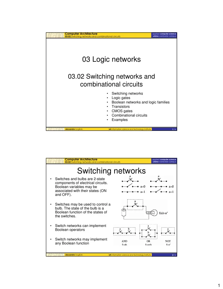
- Switching networks
- Switches and bulbs are 2-state
components of electrical circuits. Boolean variables may be associated with their states (ON and OFF).
- Switches may be used to control a
- bulb. The state of the bulb is a
Boolean function of the states of the switches.
- Switch networks can implement
Boolean operators
- Switch networks may implement
any Boolean function