
SLIDE 1
Devices (transistors, etc.) Solid-State Physics
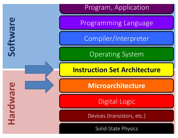
Software Programming Language Compiler/Interpreter Operating - - PowerPoint PPT Presentation
Program, Application Software Programming Language Compiler/Interpreter Operating System Instruction Set Architecture Microarchitecture Hardware Digital Logic Devices (transistors, etc.) Solid-State Physics Instruction Set Architecture
Devices (transistors, etc.) Solid-State Physics
Instruction Set Architecture (HW/SW Interface)
memory
Instruction Logic Registers
processor
Encoded Instructions Data Instructions
Local storage
Large storage
Microarchitecture (Implementation of ISA)
ALU
Registers Memory
Instruction Fetch and Decode
An example made-up instruction set architecture
Word size = 16 bits
Memory is byte-addressable, accesses full words (byte pairs). 16 registers: R0 - R15
Instructions are 1 word in size. Separate instruction memory. Program Counter (PC) register
4
Address Contents First instruction, low-order byte 1 First instruction, high-order byte 2 Second instruction, low-order byte ... ...
(HW = Hardware or Hogwarts?)
M: Data Memory R: Register File IM: Instruction Memory
Address Contents 0x0 – 0x1 0x2 – 0x3 0x4 – 0x5 0x6 – 0x7 0x8 – 0x9 … Reg Contents Reg Contents R0 0x0000 R8 R1 0x0001 R9 R2 R10 R3 R11 R4 R12 R5 R13 R6 R14 R7 R15
Program Counter PC
Address Contents 0x0 – 0x1 0x2 – 0x3 0x4 – 0x5 0x6 – 0x7 0x8 – 0x9 0xA – 0xB 0xC – 0xD …
Abstract Machine
Processor Loop
7
Assembly Syntax Meaning Opcode Rs Rt Rd ADD Rs, Rt, Rd R[d] ß R[s] + R[t] 0010 s t d SUB Rs, Rt, Rd R[d] ß R[s] - R[t] 0011 s t d AND Rs, Rt, Rd R[d] ß R[s] & R[t] 0100 s t d OR Rs, Rt, Rd R[d] ß R[s] | R[t] 0101 s t d LW Rt, offset(Rs) R[t] ß M[R[s] + offset] 0000 s t
SW Rt, offset(Rs) M[R[s] + offset] ß R[t] 0001 s t
BEQ Rs, Rt, offset If R[s] == R[t] then PC ß PC + offset*2 0111 s t
JMP offset PC ß offset*2 1000
f s e t
16-bit Encoding
(R = register file, M = memory)
LSB MSB
M: Data Memory R: Register File IM: Instruction Memory
Address Contents 0x0 – 0x1 SUB R8, R8, R8 0x2 – 0x3 BEQ R9, R0, 3 0x4 – 0x5 ADD R10, R8, R8 0x6 – 0x7 SUB R9, R1, R9 0x8 – 0x9 JMP 1 0xA – 0xB HALT Reg Contents Reg Contents R0 0x0000 R8 R1 0x0001 R9 2 R2 R10 3 R3 R11 R4 R12 R5 R13 R6 R14 R7 R15
Program Counter PC
Address Contents 0x0 – 0x1 0x2 – 0x3 0x4 – 0x5 0x6 – 0x7 0x8 – 0x9 0xA – 0xB 0xC – 0xD …
Abstract Machine
Processor Loop
Registers Memory
Instruction Fetch and Decode
Hardware implementation of the HW
Fetch instruction from memory. Increment program counter (PC) to point to the next instruction. Read Address Instruction Instruction Memory Add PC 2
12
Processor Loop
13
Instruction Meaning Opcode Rs Rt Rd ADD Rs, Rt, Rd R[d] ß R[s] + R[t] 0010 0-15 0-15 0-15 SUB Rs, Rt, Rd R[d] ß R[s] – R[t] 0011 0-15 0-15 0-15 AND Rs, Rt, Rd R[d] ß R[s] & R[t] 0100 0-15 0-15 0-15 OR Rs, Rt, Rd Rd ß R[s] | R[t] 0101 0-15 0-15 0-15 ... 16-bit Encoding Opcode Rs Rt Rd 0010 0011 0110 1000
ADD R3, R6, R8
14
Instruction
Write Data Read Addr 1 Read Addr 2 Write Addr Read Data 1 Read Data 2
ALU
ALU Op Reg Write
zero
Control Unit
ALU result
16 16 16
Register File
16 4 4 4 4 Opcode Rs Rt Rd
Write Enable
15
Instruction Meaning Op Rs Rt Rd LW Rt, offset(Rs) R[t] ß Mem[R[s] + offset] 0000 0-15 0-15
SW Rt, offset(Rs) Mem[R[s] + offset] ß R[t] 0001 0-15 0-15
...
SW R6, -8(R3)
Opcode Rs Rt Rd 0001 0011 0110 1000
16
Data Memory
Address Write Data Read Data Mem Store 32 16
Inst
Write Data Read Addr 1 Read Addr 2 Write Addr Read Data 1 Read Data 2
ALU
ALU Op Reg Write Control Unit
16 16 16
Register File
16 4 4 4 4 Sign extend 16 4
How can we support arithmetic and memory instructions? What's shared?
Opcode Rs Rt Rt Rd (offset)
Write Enable Write Enable
17
Data Memory
Address Write Data Read Data Mem Store 32 16
Inst
Write Data Read Addr 1 Read Addr 2 Write Addr Read Data 1 Read Data 2
ALU
ALU Op Reg Write Control Unit
16 16 16
Register File
16 4 4 4 4 Sign extend 16 4
Mem Load
Opcode Rs Rt Rd Rd (offset) Rt
1 1 0 1
Write Enable Write Enable
18
Instruction Meaning Op Rs Rt Rd BEQ Rs, Rt, offset If R[s] == R[t] then PC ß PC+2 + offset*2 Else PC ß PC+2 0111 0-15 0-15 offset ... 16-bit Encoding
Op Rs Rt Rd 0111 0001 0010 1110
BEQ R1, R2, -4
19
Inst
32 16 Write Data Read Addr 1 Read Addr 2 Write Addr Read Data 1 Read Data 2
ALU
ALU Op
Reg Write
Control Unit
16
16
Register File
16 4 4 4 4 Sign extend 16 4
Read Address Instruction Memory
+
PC
2 Shift left by 1
+
1 1
Write Enable
21
Inst
Data Memory
Address Write Data Read Data Mem Store 32 16 Write Data Read Addr 1 Read Addr 2 Write Addr Read Data 1 Read Data 2
ALU
ALU Op
Reg Write
Control Unit
16 16
16
Register File
16 4 4 4 4 Sign extend 16 4
Read Address Instruction Memory
+
PC
2 Shift left by 1
+
MUX
Branch?
Mem Load
1 1 0 1
Write Enable Write Enable
Single-cycle architecture
Could it be better?
22