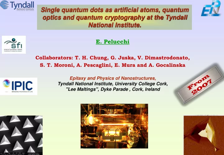
SLIDE 1
Collaborators: T. H. Chung, G. Juska, V. Dimastrodonato,
- S. T. Moroni, A. Pescaglini, E. Mura and A. Gocalinska
Single quantum dots as artificial atoms, quantum
- ptics and quantum cryptography at the Tyndall
National Institute.
Epitaxy and Physics of Nanostructures, Tyndall National Institute, University College Cork, "Lee Maltings", Dyke Parade , Cork, Ireland
SLIDE 2
Tyndall (at University College Cork)
Excellence in ICT research
SLIDE 3
Photonic Materials Device Fabrication Packaging & Integration Photonic Systems Tyndall Photonics Research Capabilities
SLIDE 4 Tyndall Photonics: a few examples
Mach-Zehnder Modulators
A
GaAs Laser Wafer Transfer printing stamp Pick-up of GaAs Chiplets Silicon Wafer Silicon Wafer Populated with GaAs Chiplets
Epitaxial material transfer Integrated DQPSK Transmitter
≥35% coupling efficiency (per grating)
AWG
Fibre coupling of Silicon photonic waveguides at Tyndall ( patent application PCT/EP2011/068240)
High speed EAM integrated with SOAs
SLIDE 5
For the moment Tyndall is the only place in Ireland with experimental quantum information work done
SLIDE 6 First Demonstration of QKD on GE-PON with simultaneous conventional data transmission
Photonic Systems: Extensive facilities (“best in europe”) Photonic Systems: Quantum information to the home
Iris Choi, Robert J Young and Paul D Townsend, New Journal of Physics 13 (2011) 063039
SLIDE 7 III-V Materials
Double reactor set-up: single w afer for high purity and 3 x2 inch for device grow ths
High purity materials
SLIDE 8
A quick reminder
SLIDE 9 Surface organization
steps organise and evolve: step bunching, steps coalescence, periodic features….
GaAs (100) surfaces with different substrate miscut An example of InP (100) 0.4° A misorientation Sand
SLIDE 10
Our single quantum dots (which sometimes are actually decent “artificial atoms”…..)
SLIDE 11 Pyramids : lithography, growth , post processing
(111)B substrate patterning; (photo)lithography+wet etching MOVPE growth: QW like Post processing to enhance extraction
“apex up” or “back etching”, prevents total internal reflection
GaAs (111)B SiO2 Photoresist (111)A InGaAs QD
SLIDE 12 (In)GaAs growth AlGaAs growth
“l “latera ral” Q ” QWs “l “latera ral” Q ” QWRs QD QD Ga Ga-rich ich A AlG lGaAs VQW QW
top v
ew side v de view ew side v de view ew
Ga Ga-rich ich AlGa GaAs s VQW QWR
System of interconnected nanostructures*
SLIDE 13 GaAs (111)B AlGaAs Etch Stop layer: Al 0.45 0.75 InGaAs QD LQWRs 100nm
InGaAs dots in GaAs barriers…
1.5 nm In0.25Ga0.75As dot in GaAs barriers
AFM cross section GaAs barriers
SLIDE 14 Purity and uniformity (typically ~4 meV)…
L.O. Mereni, V. Dimastrodonato, R.J. Young and E. Pelucchi, Appl. Phys. Lett. 94, 223121 (2009). Record linewidths for any site- controlled dots Best numbers to date, non resonant pumping, measured using interferometry: ~10 µeV
10 Kelvin!!!!
SLIDE 15 (….AlGaAs) (…GaAs) ~20 nm
This to get a nice V
How they grow…like in V-grooves quantum wires….
Lateral growth rate much stronger than on bottom Sidewalls grow faster… So called capillarity..( but may be it is capillarity, may be not…)
Attributed to
SLIDE 16 We have a model…
Ls Lb (111)A (111)B θ u1 r H
Ji + Fi = 0 , ni τi Ji = Di ni Decomposition rate anisotropy: Fs Fb r = > 1 Surface diffusion (+ “capillarity”): Di = a2 ν exp(ED
i/kBTG )
Incorporation rate: τi = Cτ exp(Eτ
i/kBTG )
Ri = = Ω0 dzi dt ni τi In 3D… (similarly in 2D): it gives 2D diffusion , which one solves for stationary solution putting appropriate boundary conditions (111B/111A)
- V. Dimastrodonato, E. Pelucchi, and D. D. Vvedensky, “Self-limiting profile evolution of seeded two-
and three- dimensional nanostructures during metalorganic vapour-phase epitaxy”, Phys. Rev. Lett. 96, 130501 (2012).
Precursors decomposition only appear as an extra deposition flux, F…
SLIDE 17 Pyramids…self limited profile prediction Note: much more difficult the VQWR concentration
T = 938 K T = 938 K Al
- V. Dimastrodonato, E. Pelucchi, and D. D. Vvedensky, “Self-limiting
profile evolution of seeded two- and three- dimensional nanostructures during metalorganic vapor-phase epitaxy”, Phys. Rev. Lett. 96, 130501 (2012).
SLIDE 18 Al0.3Ga0.7As
TG
Al0.3Ga0.7As
Self-limited regime: growth temperature
SLIDE 19 Al0.55Ga0.45As Al0.8Ga0.2As
Self-limited regime: Ga segregation
T = 938 K T = 938 K T = 938 K T = 938 K Ga Nom = 0.2 Ga Nom = 0.4 Ga Nom = 0.6 Ga Nom = 0.8 T = 938 K T = 938 K
GaEff
=
k (1-xAl) k (1-xAl) + xAl
SLIDE 20
We can reproduce also InGaAs in V-grooves
Stefano Moroni et al., Journal of Applied Physics 117, 164313 (2015). Original figure from Lelarge et al., Applied Physics Letters 75, 3300 (1999): only the TEM model is original
SLIDE 21
Why it is not too bad to call QDs artificial atoms….
SLIDE 22 So, entangled photons….not our idea..since dots are “artificial atoms”…
BiExcitonic State: 2X, two degenerate levels antisimmetricly arranged Excitonic State: X Ground State
One can use the transition from a “singlet state” (an “entangled” state because of indistinguishability, text book physics) It has been done with real atoms in the early seventies..
Just considering the two electrons Two exchangeable electrons, and two exchangeable holes… appropriate parity under particle exchange
SLIDE 23 Parenthesis…
It is clear from what I said that a biexciton (and not only one confined in a dot) is not a separable state
(D. A. Kleinman Phys. Rev. B 28, 871 (1983) and many more) XX: X:
Ground level FSS
Bright States
2x
And… the which path information story….at the beginning the community sort of “were puzzled”.. because of asymmetry: must be a which path information (the jargon used)
XX:
Ground level Just the electrons…
SLIDE 24 Long story short if you have FSS…
+ = VV HH
e h FSS i / 2
2 1
τ π
ψ
- R. Mark Stevenson et al. Phys Rev. Lett. 101, 170501 (2008)
When a FSS splitting is present the state tomography procedure averages over several randomly distributed/emitted different entangled states, practically resulting in an apparent classical state.…. one is left with a statistical mixture…
SLIDE 25
Rigorously, and outside specialized scientific jargon, in each specific repetition of the experiment there is no “which path” information in the cascade process, as only after the first photon is measured, the superposition entangled state is projected onto a specific polarization and energetic state The process has, for this reason, no real similarity with a “double slit“ experiment where the slit the photon has gone through is where a “which path” information obtained by some extra/external measurement can be effectively obtained. It would, on the other hand, have resemblances, if any, with the phenomenon of coherence loss caused by random phases. (ref. M.O. Scully, B. Englert and H. Walter, Nature,351, 6322 (1991))
During the cascade and the “flying” period, it stays as an entangled state
SLIDE 26 So, long story short: it is easier with a symmetric dot to “see “ the entanglement
XX: X:
m=1 m=-1 m=-2 m=2
XX: X:
Ground level FSS
Bright States
Pyramids should have C3V symmetry which should ensure suppression of the FSS.
Singh, R., et al. Phys. Rev. Lett., 2009, 103(6), Schliwa, A., et al. Phys. Rev. B, 2009, 80(16), Karlsson, K.F., et al. Phys. Rev. B, 2010, 81(16).
FSS FSS
Low temperature grown, 1.2 nm InGaAsN QD: 90 µeV
2x
SLIDE 27 In0.25Ga0.75As1-εNε… some interesting unexpected features
Measuring the fine structure splitting…. …..
This is unusual, we normally have some splitting (i.e. X and XX photons are linearly polarized.. not circularly polarized as they would be in a perfectly symmetric system)
Difference in energy between the exciton and the biexciton for
- ne dot plotted as a function of the half wave plate angle, in a
standard InGaAs (no nitrogen) and In0.25Ga0.75As1-εNε dots
Symmetric dot Asymmetric dot
With Hydrazine No Hydrazine
SLIDE 28 APD APD
HBT correlator:
Spectrometer 1 START STOP CCD PBS x4 HXX VXX 50:50 Spectrometer 2 APD PBS HX VX APD … … g(2)(t)
λ/2/4
( )
V i H R + =
2 1
( )
V i H L − =
2 1
( )
V H D + =
2 1
( )
V H A − =
2 1
( ) ( ) ( )
X XX X XX X XX X XX X XX X XX
A A D D V V H H L R R L + = = + = = + =
2 1 2 1 2 1
ψ
6/12
Area A Area B
( )
X XX X XX
L R R L +
2 1
Fidelity to the expected maximally entangled state:
- G. Juska et al. , Nature Photonics 7, 527, 2013
Polarization-entangled photon emission
SLIDE 29
Can we electrically inject?
If you think about it, it should not work….. Current prefers to go through the sides…shorter path (a factor of 3 or so!!!)..
SLIDE 30 Apex-up geometry is essential to ensure high light extraction efficiency. Issues:
- Non-planar structure
- Current leakage outside QD region
Device fabrication….issues
SLIDE 31
How to make it work… engineered injection…VQWR..
SLIDE 32 Vertical Quantum Wire (VQWR) – gallium segregated, self-formed nanostructure going along the center of a pyramid.
p n
GaAs 10 nm Al0.3GaAs 30 Al0.75GaAs 45 GaAs 60 In0.25GaAs 0.55 GaAs 90 Al0.75GaAs 45 GaAs 60 Al0.8GaAs 90 Al0.45~0.8GaAs 45 GaAs 40 nm
Simulation of current density distribution within the pyramid-like structure.
Selective injection of QDs
SLIDE 33
- 2. Evaporation of Si3N4
- 3. Angle evaporation of the mask metal
- 4. Opening Si3N4 aperture
- 5. Evaporation of the bottom contact
- 8. Evaporation of the top contact
- 1. Growth of the p-i-n structure
- 7. Substrate etching
p n i
- 6. Bonding the supporting substrate
LED production steps:
Au Au
V
7/12
Diode processing
SLIDE 34 8/12
25 μm
Electroluminescence
SLIDE 35
- A single QD electro-luminescence
<FSS> = 2.9±1.8 μeV
- FSS values
- Functional μLED distribution and
FSS values
Symmetry
SLIDE 36 Fidelity of unpolarized source: Degree of correlation: F = 0.69±0.06 F = 0.85±0.04
Entangled photon emission
SLIDE 37
- Pulsed injection:
- Correlations:
- Simplified estimations of Bell’s inequality:
(Young, R. J. PRL 102, 030406,2009)
( )
2 2 ≤ + =
D R RD
C C S
( )
2 2 ≤ − =
C D DC
C C S
( )
2 2 ≤ − =
C R RC
C C S
( ) ( )
) 2 ( , ) 2 ( , ) 2 ( , ) 2 ( , x xx x xx x xx x xx basis
g g g g C + − =
With 1.5 ns window and 75% intensity preserved: SRD=2.053±0.070 SDC=2.191±0.075 SRC=2.239±0.074
Triggered entangled photon emission
SLIDE 38 Adding local metallic contacts:
- Electric injection of carriers.
- Tuning emission energy.
- Tuning the fine-structure splitting.
- Electrical manipulation of spins.
Integration of QDs on piezoelectric actuators:
- Tuning emission energy.
- Tuning the fine-structure splitting.
Collaboration with JKU Linz (A. Rastelli, R. Trotta, et al.) 11/12
Short term future
SLIDE 39
Back to surfaces…
SLIDE 40
Al48%In52%As (2 nm) on InP
Normally..
SLIDE 41
A different way of growing dots..
InP on Al48%In52%As
SLIDE 42 A different way of growing dots..II
AFM morphologies (signal amplitudes) and corresponding zoom-in 3D reconstructions of 1nm InP layer deposited on LM AlInAs after 5sec mixed AsH3 and PH3 growth interruption. Samples grown on SO = (100) at T = 630 °C, Gr = 0.7 µ/h, V/III = 180 and then a) immediately cooled down under PH3, b)exposed to AsH3 at growth temperature for 5 minutes and then cooled down under PH3, c) exposed to AsH3 at growth temperature for 1 minute and then cooled down under AsH3.
SLIDE 43 Interesting emission
Part of the low temperature photoluminescence spectrum of nominally 1 nm InP in In0.9Ga0.1P and Al0.48In0.52As barriers, after exposing the QDs layer to arsine overflow. Top left insert shows zoom in to the spectrum detail with FWHM stated for each line, top central and right inserts show power dependence of the peak intensity, allowing for identification of the individual peaks as corresponding to exciton (X) and biexciton (XX) transitions.
SLIDE 44
And we….the quantum snout
SLIDE 45
Thanks