seq part 2
play

SEQ part 2 muxes to make decisions (dont bother memorizing their - PowerPoint PPT Presentation

SEQ part 2 muxes to make decisions (dont bother memorizing their mnemonics) what they are note: if we ever use shift instructions on a test, we will tell you the correct mnemonic is sar on some other architectures (e.g. MIPS), but not on x86


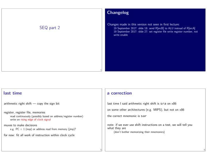
  1. SEQ part 2 muxes to make decisions (don’t bother memorizing their mnemonics) what they are note: if we ever use shift instructions on a test, we will tell you the correct mnemonic is sar on some other architectures (e.g. MIPS), but not on x86 last time I said arithmetic right shift is sra on x86 a correction 5 for now: fjt all work of instruction within clock cycle e.g. PC + 1 (nop) or address read from memory (jmp)? write on rising edge of clock signal 1 read continuously (possibly based on address/register number) register, register fjle, memories arithmetic right shift — copy the sign bit last time 1 write enable 19 September 2017: slide 27: set register fjle write register number, not 19 September 2017: slide 18: send R[srcB] to ALU instead of R[srcA] Changes made in this version not seen in fjrst lecture: Changelog 6

  2. arithmetic right shift the question this week PC input — yes; need to handle instruction length register #/value to write — yes (either one); don’t change register on nop register number for “none” (15) or new value = old value instruction memory address — no; always equal to PC output 9 jmp+addq+mrmovq register to read — no; read and ignore result on nop read reg. # — no; read and ignore for jmp PC input — yes; varibale instruction length, jumps write reg. # — need MUX on this or register value input write enable for memory — no; hard-wire to false address input to instruction memory — no; equal to PC output ALU inputs — yes; mrmovq needs to add constant from instruction but ‘cleaner’ to specify no register explicitly?? nop+add — where do we need a MUX (or similar logic)? 10 “How on earth do you except us to answer a similar question on the (((unsigned char)200) >> 3) == 25 (logical: the question last week anonymous feedback (1) 7 quiz as the fjnal example during class, to which you gave a half-explained answer? …” (paraphrased:) and your explanation didn’t give a yes/no answer to yes/no questions 8 logical right shift — add zeroes 1011000 → 0101100 arithmetic right shift — copy sign bit 1011000 → 1101100 ( x >> 1) ≈ x / 2 even for signed ( x >> 2) ≈ x / 4 even for signed ( x >> 3) ≈ x / 8 even for signed ((-56) >> 3) == -7 (arithmetic: 11001000 → 11111001 ) 11001000 → 00011001 )

  3. anonymous feedback (2) really should be no obligation to do more than assignment says (paraphrased) please check your slides more carefully anonymous feedback (4) 13 I think this policy would create some perverse incentives wrong on the quizzes (paraphrased) you should drop any question most students get anonymous feedback (4) 12 But better ways of making it feel optional? (paraphrased) the question on timing on the post-quiz was unfair I like it better than extra credit because it’s more optional competitions make some of our students learn more intimidating/demoralizing (paraphrased) competition scoreboard for bomb HW was anonymous feedback (3) 11 (but, yes, easier if you had read ahead) intention: how addq CPU + register fjle + registers worked since it was in next week’s textbook material 14

  4. lists HW +2 Mem. ZF/SF Data in Addr in Data out split MUX convert opcode immediate + (ALU) +10 next R[dstM] rrmovq rA, rB 2 0 rA rB irmovq V, rB 3 0 F rB mrmovq D(rB), rA 5 0 rA rB V D Data dstM due tommorrow irmovq $constant, %rYY hopefully you’ve started — don’t fjght segfaults at the last minute 15 bit puzzles lab/HW bit fjddling problems, e.g. isLessThanOrEqual all in C restrictions on operators you can use lab — practice problems, complete what you can N.B.: you can work together uneven diffjculty; don’t expect anyone to do all of them 16 simple ISA 4: mov-to-register rrmovq %rXX, %rYY next R[dstE] mrmovq 10(%rXX), %rYY 17 mov-to-register CPU PC Instr. Mem. register fjle srcA srcB R[srcA] R[srcB] dstE 18 homework — difgerent problems, complete all

  5. mov-to-register CPU irmovq V, rB immediate + (ALU) +2 +10 rrmovq rA, rB 2 0 rA rB 3 convert 0 F rB mrmovq D(rB), rA 5 0 rA rB V D opcode MUX mov-to-register CPU next R[dstE] Mem. register fjle srcA srcB R[srcA] R[srcB] dstE dstM split next R[dstM] Data Mem. ZF/SF Data in Addr in Data out 18 PC PC irmovq V, rB immediate + (ALU) +2 +10 rrmovq rA, rB 2 0 rA rB 3 convert 0 F rB mrmovq D(rB), rA 5 0 rA rB V D opcode MUX Instr. next R[dstE] Mem. register fjle srcA srcB R[srcA] R[srcB] dstE dstM split next R[dstM] Data Mem. ZF/SF Data in Addr in Data out Instr. mov-to-register CPU PC 0 rA rB opcode immediate + (ALU) +2 +10 rrmovq rA, rB 2 irmovq V, rB MUX 3 0 F rB mrmovq D(rB), rA 5 0 rA rB V convert split 18 dstE Instr. Mem. register fjle srcA srcB R[srcA] R[srcB] next R[dstE] Data out dstM next R[dstM] Data Mem. ZF/SF Data in Addr in D mov-to-register CPU 18 irmovq V, rB immediate + (ALU) +2 +10 rrmovq rA, rB 2 0 rA rB 3 convert 0 F rB mrmovq D(rB), rA 5 0 rA rB V D opcode MUX PC dstE Instr. Mem. register fjle srcA srcB R[srcA] R[srcB] next R[dstE] split dstM next R[dstM] Data Mem. ZF/SF Data in Addr in Data out 18

  6. mov-to-register CPU mov-to-register CPU next R[dstM] dstM next R[dstE] dstE R[srcB] R[srcA] srcB srcA register fjle Mem. Instr. PC 18 Mem. D V 0 rA rB 5 mrmovq D(rB), rA F rB 0 3 irmovq V, rB 0 rA rB 2 rrmovq rA, rB +10 Data ZF/SF + (ALU) 3 rmmovq %rXX, 10(%rYY) mrmovq 10(%rXX), %rYY rrmovq %rXX, %rYY irmovq $constant, %rYY simple ISA 4B: mov 18 D V 0 rA rB 5 mrmovq D(rB), rA F rB 0 irmovq V, rB Data in 0 rA rB 2 rrmovq rA, rB +10 +2 + (ALU) immediate opcode convert MUX split Data out Addr in +2 immediate PC Data in 0 rA rB 2 rrmovq rA, rB +10 +2 + (ALU) immediate opcode convert MUX split Data out Addr in ZF/SF 3 Mem. Data next R[dstM] dstM next R[dstE] dstE R[srcB] R[srcA] srcB srcA register fjle Mem. Instr. irmovq V, rB 0 opcode R[srcB] convert MUX split Data out Addr in Data in ZF/SF Mem. Data next R[dstM] dstM next R[dstE] dstE R[srcA] F rB srcB srcA register fjle Mem. Instr. PC mov-to-register CPU 18 D V 0 rA rB 5 mrmovq D(rB), rA 19

  7. mov CPU write enable MUX convert opcode immediate immediate + +2 +10 0xF from convert opcode Data out rrmovq rA, rB 2 0 rA rB irmovq V, rB 3 0 F rB mrmovq D(rB), rA 5 0 rA rB split Addr in 4 register fjle valB valA valE valM 20 mov CPU PC Instr. Mem. srcA Data in srcB R[srcA] R[srcB] dstE next R[dstE] dstM next R[dstM] Data Mem. ZF/SF rmmovq rA, D(rB) 0 rA rB valP + (ALU) Data in Addr in Data out split MUX convert opcode immediate immediate +2 Mem. +10 0xF write enable from convert opcode fetch decode execute memory writeback PC update ZF/SF Data V mov CPU D D valP valC valB valA valE valM 20 PC next R[dstM] Instr. Mem. register fjle srcA srcB R[srcA] R[srcB] dstE next R[dstE] dstM valC D PC 0 +10 0xF write enable from convert opcode rrmovq rA, rB 2 0 rA rB irmovq V, rB 3 F rB + mrmovq D(rB), rA 5 0 rA rB rmmovq rA, D(rB) 4 0 rA rB V D D valP +2 immediate valB dstM Instr. Mem. register fjle srcA srcB R[srcA] R[srcB] dstE next R[dstE] next R[dstM] immediate Data Mem. ZF/SF Data in Addr in Data out split MUX convert opcode valC valA D 0 rA rB immediate + +2 +10 0xF write enable from convert opcode rrmovq rA, rB 2 irmovq V, rB opcode 3 0 F rB mrmovq D(rB), rA 5 0 rA rB rmmovq rA, D(rB) 4 0 rA rB V immediate convert valE R[srcB] valM 20 mov CPU PC Instr. Mem. register fjle srcA srcB R[srcA] dstE MUX next R[dstE] dstM next R[dstM] Data Mem. ZF/SF Data in Addr in Data out split 21

  8. mov CPU 2. memory changes 1; then 2, 3, and 4 at almost the same time b. 1; then 2, 3, and 4 in any order a. Hint: recall how registers, register fjles, memory works 4. PC changes 3. %rsp changes 1. instruction read 1; then 2; then 3; then 4 Order when these events happen pushq %rax instruction: fetch / decode / execute / memory / write back / PC update stages and time 22 PC update — compute next value of PC write back — write to register fjle PC c. d. decode — read register fjle decode input wire to PC register name of a wire from instruction memory part of output wires PC update write back memory fetch 1; then 3; then 2; then 4 nop stage stages example: nop 23 something else f. 1; then 2; then 3 and 4 at almost the same time e. execute — arithmetic (including of addresses) memory — read or write data memory fetch — read instruction memory, split instruction, compute length next R[dstE] Addr in Data in ZF/SF Mem. Data next R[dstM] dstM dstE split R[srcB] R[srcA] srcB srcA register fjle Mem. Instr. conceptual division of instruction: Data out MUX convert Stages 21 PC update writeback memory execute decode fetch 24 from convert opcode write enable 0xF +10 +2 + (ALU) immediate immediate opcode icode : ifun ← M 1 [ PC ] valP ← PC + 1 ← means putting a value on a wire ← means putting value on PC ← valP

Download Presentation
Download Policy: The content available on the website is offered to you 'AS IS' for your personal information and use only. It cannot be commercialized, licensed, or distributed on other websites without prior consent from the author. To download a presentation, simply click this link. If you encounter any difficulties during the download process, it's possible that the publisher has removed the file from their server.

Recommend


More recommend