
SLIDE 1
scintillator CAL for Linear Collider
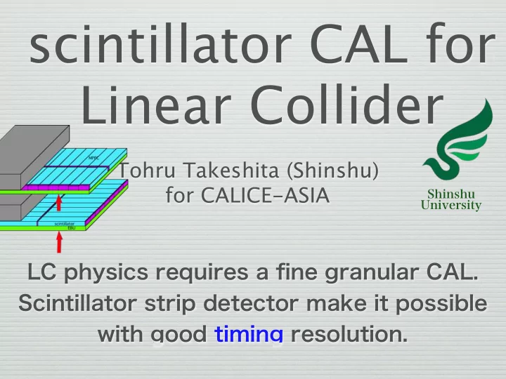
Tohru Takeshita (Shinshu) for CALICE-ASIA LC physics requires a fine granular CAL. Scintillator strip detector make it possible with good timing resolution.
Shinshu University
scintillator CAL for Linear Collider Tohru Takeshita (Shinshu) for - - PowerPoint PPT Presentation
LC physics requires a fine granular CAL. Scintillator strip detector make it possible with good timing resolution. Shinshu University scintillator CAL for Linear Collider Tohru Takeshita (Shinshu) for CALICE-ASIA scintillator strip for
Tohru Takeshita (Shinshu) for CALICE-ASIA LC physics requires a fine granular CAL. Scintillator strip detector make it possible with good timing resolution.
Shinshu University
n scintillator is robust, reliable and stable
for calorimeter sensor
n to meet PFA requirement which is fine
granularity
n perpendicular strips make it possible, n while keeping the number of readout
channel rather reduced (than pad/pixel type)
n with novel silicon-photo-detector n issue: uniformity, light yield and
dynamic range as a calorimeter
45x5x2mm3 2.45x1.9x0.85mm3
n measured in lab. by beta rays n in front of the sensor, too much direct lights
45mm 5mm light yield
present design naked
with reflector Tsuzuki
key : air gap and reflector
n Geant4 simulation (not optimized)
slc : parameter of reflection Tsuzuki direct light
n we need reflector &
air gap
n if we spatter Al on the
scintillator surface
Al spattering present des
n measured by beta rays n different thickness 1 ~ 2 mm n well separated from noise
Hamasaki
n ECAL will have Bhabha events which
generate maximum shower energy
n simulation of 250GeV electrons
1700 MIP energy / sc-strip (5x45mm2)
dE /strip (GeV)
500 1000 1500 2000 50 100 150 200 250 300
strip scintillator energy deposit (MIP)
Emax(MIP)Emax(MIP)
Egamma(GeV)
if 7p.e./MIP ~10000 pixel
Incident Photon Intensity [photoelectrons on MPPC] 2000 4000 6000 8000 10000 MPPC output [p.e.] 500 1000 1500 2000 2500 3000 3500 4000
10000pix_75.084V 4400pix_69.522V 1600pix_67.031VComparison of RC
n Pixelated PD response is limited by its number
n to measure BhaBha EM shower n max. pixel needed ~ 10000, when a mip ~7 p.e. n slow saturation is seen due to time structure
n metal register n 10kpix./1mm2
10k 1.6k 10um
n PPD has dead volume in the
scintillator area
n to avoid it, surface mounted PPD
should collect lights, how ?
simulation
tapered wedge wedge present
normal sensor location
by S.Ieki(Tokyo)
n by beta rays n normal n tapered wedge n wedge
1.5mm
n optimize PPD location and size
width direction[mm] distance form end of wedge width direction[mm] distance form end of wedge
simulation simulation
wider PPD square PPD
strip center strip center
x x x x
0.25mmx4mm PPD 1mmx1mm PPD
n current status n strip: 5mm x 45mm x 2mm
thick
n 144 ch./layer of 18cm
x18cm
n front end electronics
embedded
n 4 SPIROCs (4x36ch) n EBU (Ecal Base Unit)
144 strips on a EBU terminal EBU 180 mm 180 mm middle EBU 180x180mm2board
n 36ch/ASIC chip made
by Omega
n bias V control n 12bit ADC with dual
gains
n auto-trigger mode n external trigger and
validation bit
n 12bit TDC with < 1ns
n LED lights go through a
hole for each strip
n 92% success
ADC cont
200 250 300 350 400 450 500 550 600Entries
20 40 60 80 100ChipID==132&&ChannelNumber==18&&Trigger==13
h1 Entries 7000 Mean 304.6 RMS 37.62 / ndf 2ChipID==132&&ChannelNumber==18&&Trigger==13
Forward layer result @DESY
can be carried out at lab.
193 194 195 196
n by Sr90 e-source, with auto-trig. mode
稲吉 信州 Source Test
129 130
MPPC への InPut DAC を変更
反応しない イカレタ信号 肩 分離は難
90Sr
good for mass test
n at DESY n two EBU types: M & T n synchronized DAQ with n AHCAL (SPIROC) n SiECAL (SKYROC) n
Middle EBU Terminal EBU
AHCal layer Sc layer
beam
Si layer Sc layer
beam
n 3GeV electrons n auto-trigger mode +
external validation mode
n pedestal subtracted well n success 98% & 96%
ADC counts
300 400 500 600 700 800 900
Entries
200 400 600 800 1000 1200
0.5 mip threshold 8 p.e. No signal. strange signal (noisy) is difficult to separate. But get the MPV.
ch5 forward backward
100 200 300 400 500 600 20 40 60 80 100 120 140 160 180 200 Run_208 ChipID_196 Ch_14 2.38 ± ADC/MIP = 131.7 = 1.15 Entry = 5323 2193 194 195 196 225 228 227 226
TDC_Dif
Entries 481 Mean 285.3 RMS 355.5
1000 2000 3000 4000 10 20 30 40 50
TDC_Dif
Entries 481 Mean 285.3 RMS 355.5
TDC_Chip225 Entries 481 Mean 1620 RMS 577.7 TDC_Chip225 Entries 481 Mean 1620 RMS 577.7 TDC_Chip194 Entries 481 Mean 1334 RMS 450 TDC_Chip194 Entries 481 Mean 1334 RMS 450
Max.TDC_Dif: 1739TDC_dif
R488-Layer1Ch2&Layer2Ch32coincidence
の ありの で: 1層だけみれば、形はほぼ同じ。 1層と2層の差を見れば、形は色々あります 上二つの図では: による、 の 差の が違う
******************************************************************
difg. L1 L2
n timing
information for each channel
n difference ~0 n resolution ~2ns/
ch.
n with simple SSA, we have
5mm x 5mm resolution
n almost consistent with lab.
stand alone test
Section0 Section8
Position scan with beam MPPCs
Section Point
2 4 6 8 10
N_P.E.
2 4 6 8 10 12
Chip194Ch23 Chip194Ch24 Chip194Ch25 Chip194Ch26
Uniformity
Section Point
2 4 6 8 10
N_P.E.
2 4 6 8 10 12
Chip226Ch23 Chip226Ch24 Chip226Ch25 Chip226Ch26
Uniformity
Section Section Np.e. Np.e.
Scintillator
Forward layer Np.e. Backward layer Np.e.
Scintillator
0.01 0.02 0.03 0.04 0.05 0.06 0.07 0.08 0.09 0.1
X Axis
20 40 60 80 100 120 140 160 180
Y Axis
20 40 60 80 100 120 140 160 180 0.01 0.02 0.03 0.04 0.05 0.06 0.07 0.08 0.09 0.1
X Axis
20 40 60 80 100 120 140 160 180
Y Axis
20 40 60 80 100 120 140 160 180
n simple SSA applied
EBU layers covered by sheet Tungsten plates
3Wplates 7Wplates
Cell Energy
backward layer
n diagonal settings in
AHCAL
n similar but finer
correlation
1 5 9 9 1 8 7 21 18 12 8 1 1 7 7 5 7 1 105 34 12 3 6 3 6989 255 24 4 3 17 4 4473 10 1 10 6 6 16 3 1 1 1 10 7 12 3 3 2 2 7 2 5 8 6 1 1 13 1X Axis
50 100 150 200 250 300 350
Y Axis
50 100 150 200 250 300 350 100 200 300 400 500 600 HitRateDisplay_HBU_with_twoLayers
High Threshold High Threshold H it M ap o f H BU High Threshold High Threshold
6 17 5 3 1 2 1 5 16102937272528152317 4 4 3 1 7 3 10 7 19213958666162152217 3 5 2 3 1 5 12395463 134 197 171 12226502212 6 2 1 2 183762 104 124 240 394 350 28055924012 2 1 5 1 2 2046 112 204 254 450 720 653 53683 1634514 6 4 1 2 2 32 105 218 471 584 591 707 622 36365 128391513 2 6 1 2 42 169 423 793 1022 710 405 390 2993566342114 2 4 4 4 37 145 356 693 876 541 324 319 25342622613 3 1 1 2 2 1781 199 372 559 308 1179861161410 2 3 1 2 1386 187 325 475 253918775231513 3 5 3 3 175685 166 234 123574431131711 7 1 2 1 4 2232579365242820 8 10 3 4 4 3 1 1 6 1316233913101110 4 7 2 1 2 2 1 9 11112843291110 8 3 1 5 2 2 2 1 3 5 3 2 2 2 2 1 3 2 7 9 10 5 3 2 5 3 3 1 1 2 1 3 3 1010 3 6 2 1 3 2 2 2 1 1 1X Axis
20 40 60 80 100 120 140 160 180Y Axis
20 40 60 80 100 120 140 160 180 200 400 600 800 100 HitRateDisplay_EBU_with_twoLayersHigh Threshold High Threshold High Threshold
18cm 18cm 18cm 18cm
H it M ap o f EBU
n fine segmented scintillator strip ECAL is under
developing with good timing resolution
n strip has become homogeneous enough,
without dead space by PPD
n 1mm thick scintillator is under consideration n embedded FEE is developing with LED &
source calibration capability in lab. by auto- trigger
n power pulsing test n combined DAQ with silicon ECAL/AHCAL
n a calorimeter with
homogeneous structure
n tungsten absorbers and
scintillator sensors
n need long slav
construction and test
EBU
Thinner EBU can reduce thickness of ECAL ▶ Developed by AHCAL group 1.8 mm ▶ 1.2-1.3 mm req. ASIC package Total Compress 0.6 mm, ex Ball grid array w/ naked ASIC
Further optimization (1) :thickness of EBU
Ecal Base board Unit (EBU)
Small radius of magnet ▶ Lowcost
25
n ADC/MIP constants are
systematically shifted
n reasons are under
investigation
50 100 150 200 250 300 10 20 30 40 50
chip193 chip194 chip195 chip196
Reject Dead and NoisyPreliminary #136Chs,mean=115.6,RMS=26.5
scfactor_forward
Forward layer ADC/MIP
50 100 150 200 250 300 10 20 30 40 50
chip225 chip226 chip227 chip228
Reject Dead and NoisyPreliminary #118Chs,mean=159.7,RMS=29.7
scfactor_backward
Backward layer ADC/MIP
n 16 analog memory cells/ch n they are difgerent with pedestals
c0
Entries 4876 Mean 276 RMS 4.72230 240 250 260 270 280 290 300 310 320 50 100 150 200 250 300 350 400
c0
Entries 4876 Mean 276 RMS 4.72 ADCData {ChipID==195&&ChannelNumber==2&&MemoryCell==0} c1 Entries 4534 Mean 278.4 RMS 5.014 c1 Entries 4534 Mean 278.4 RMS 5.014c2
Entries 4467 Mean 263.1 RMS 6.135c2
Entries 4467 Mean 263.1 RMS 6.135c3
Entries 4043 Mean 255.8 RMS 6.398c3
Entries 4043 Mean 255.8 RMS 6.398 c4 Entries 3843 Mean 254.7 RMS 6.351 c4 Entries 3843 Mean 254.7 RMS 6.351c5
Entries 3229 Mean 262 RMS 5.833c5
Entries 3229 Mean 262 RMS 5.833c6
Entries 2815 Mean 275.8 RMS 5.163c6
Entries 2815 Mean 275.8 RMS 5.163c7
Entries 2164 Mean 272.2 RMS 4.986c7
Entries 2164 Mean 272.2 RMS 4.986c8
Entries 1688 Mean 272.4 RMS 5.069c8
Entries 1688 Mean 272.4 RMS 5.069c9
Entries 1161 Mean 265.6 RMS 6.181c9
Entries 1161 Mean 265.6 RMS 6.181c10
Entries 784 Mean 266.5 RMS 6.038c10
Entries 784 Mean 266.5 RMS 6.038c0
Entries 7000 Mean 273.4 RMS 7.215230 240 250 260 270 280 290 300 310 320 100 200 300 400 500 600
c0
Entries 7000 Mean 273.4 RMS 7.215 ADCData {ChipID==195&&ChannelNumber==2&&MemoryCell==0}c1
Entries 7000 Mean 270.1 RMS 8.763c1
Entries 7000 Mean 270.1 RMS 8.763c3
Entries 7000 Mean 266.6 RMS 10.2c3
Entries 7000 Mean 266.6 RMS 10.2 c4 Entries 7000 Mean 271.8 RMS 9.013 c4 Entries 7000 Mean 271.8 RMS 9.013c5
Entries 7000 Mean 266.8 RMS 7.83c5
Entries 7000 Mean 266.8 RMS 7.83 c6 Entries 7000 Mean 266.4 RMS 7.754 c6 Entries 7000 Mean 266.4 RMS 7.754 c7 Entries 7000 Mean 274.7 RMS 9.198 c7 Entries 7000 Mean 274.7 RMS 9.198 c8 Entries 7000 Mean 275.3 RMS 9.863 c8 Entries 7000 Mean 275.3 RMS 9.863c2
Entries 7000 Mean 273.1 RMS 19.78c2
Entries 7000 Mean 273.1 RMS 19.78Run185_Channel2 Run159_Channel2