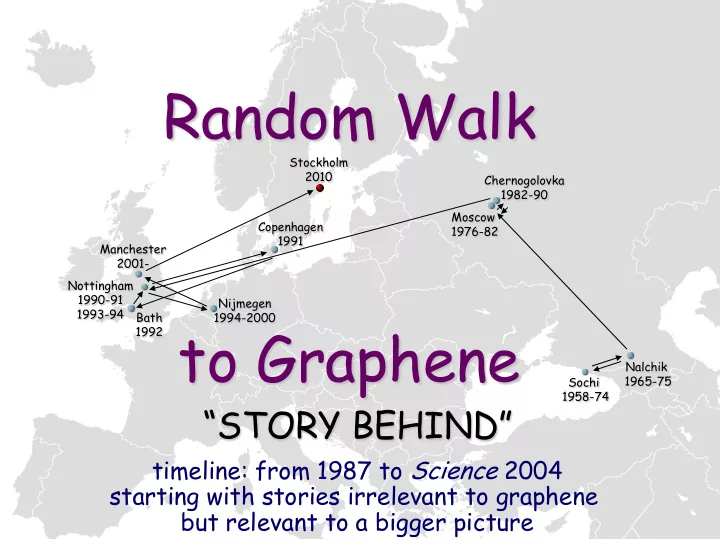
random walk
play

Random Walk Stockholm 2010 Chernogolovka 1982-90 Moscow - PowerPoint PPT Presentation

Random Walk Stockholm 2010 Chernogolovka 1982-90 Moscow Copenhagen 1976-82 1991 Manchester 2001- Nottingham 1990-91 Nijmegen 1993-94 Bath 1994-2000 to Graphene 1992 Nalchik 1965-75 Sochi 1958-74 STORY BEHIND timeline:


  1. Random Walk Stockholm 2010 Chernogolovka 1982-90 Moscow Copenhagen 1976-82 1991 Manchester 2001- Nottingham 1990-91 Nijmegen 1993-94 Bath 1994-2000 to Graphene 1992 Nalchik 1965-75 Sochi 1958-74 “STORY BEHIND” timeline: from 1987 to Science 2004 starting with stories irrelevant to graphene but relevant to a bigger picture

  2. PhD 1987 “Investigation of mechanisms of transport relaxation in metals by a helicon resonance method” message I took away: NEVER TORTURE STUDENTS WITH BORING/DEAD PROJECTS ! as exciting as it sounds

  3. SWEET TASTE OF FREEDOM staff scientist in Chernogolovka: 1988-1990 something new but still possible diffusive with available Soviet facilities ballistic magnetic field inhomogeneous on a submicron scale experience I took away: NEW EXPERIMENTAL SYSTEM Geim , JETP Lett. 1989 IS BETTER THAN Geim, Sergey Dubonos et al A NEW PHENOMENON ! JETP Lett. 1990 later, two PRL 1991, 1994

  4. MOVING YEARS age =32 h -index ~1 postdocs in Nottingham x2, Bath & Copenhagen: 1990-1994 SEMICONDUCTOR PHYSICS my first 6-month visit submicron GaAs wires from a drawer Geim, Laurence Eaves, Peter Main et al Phys. Rev. Lett. 1991 Phys. Rev. Lett. 1992 GaAlAs heterostructures experience to tease colleagues: universal conductance fluctuations “NO SUCH THING resonant tunnelling phenomena quantum point contacts AS BAD SAMPLES, quantum Hall effect ONLY BAD POSTDOCS  ” 2DEG in periodic potentials

  5. GOING DUTCH associate professor in Nijmegen: 1994-2000 FINDING RESEARCH NICHE: MESOSCOPIC possible but somewhat different SUPERCONDUCTIVITY micron-sized Hall probes to investigate paramagnetic Meissner effect superconductors, ferromagnetics, etc T > T C T < T C fractional flux vortices & vortex shells structures from Nottingham lithography in Russia: Sergey Dubonos measurements in Nijmegen writing up with Irina Grigorieva: Nature 390 , 259 (1997); Nature 396 , 144 (1998); Nature 407 , 55 (2000); PRL 79 , 4653 (1997); PRL 85 , 1528 (2000)

  6. “FRIDAY NIGHT EXPERIMENTS” starting 1997 water in high magnetic fields? magnetic water descaler ancient magnets: consume a lot of energy require extra cryostats

  7. A BIT OF LEVITY water in high magnetic fields

  8. NEEDS EMPHASIS Nature 1991

  9. KNOWLEDGE IS FUN

  10. WOW! FACTOR

  11. PERCEPTION CHANGE everything (and everybody) is magnetic; ever present diamagnetism is NOT negligible messages to take away: LOOK FOR COMPETITIVE EDGE even obsolete facilities may offer some sideline experience of the IgNobel Prize: in many textbooks DON’T TAKE YOURSELF TOO SERIOUSLY

  12. MANCUNIAN WAY chair in Manchester: 2001 – present empty lab; little start-up; no central microfabrication FIRST ESTABLISH YOURSELF & SET UP NEW FACILITIES microfabrication still in Russia ( Dubonos ) 2 µ m Au probes on top of 2DEG rings 2DEG-ferromagnetic- -superconducting hybrid 1 µ m V H I Kostya Novoselov et al, Nature 426 , 812 (2003) Irina Grigorieva et al, PRL 92 , 237001 (2004) by 2003: well-equipped lab and state-of-the-art microfabrication thanks to EPSRC & University subatomic movements of domain walls

  13. “FRIDAY NIGHTS” in MANCHESTER HOW COMES THAT GECKO CAN CLIMB WALLS?

  14. “FRIDAY NIGHTS” in MANCHESTER sticky feet: geckos climb due to their hairy toes courtesy of K Autumn PNAS 2002 submicron size (!) - standard spatial scale in our work

  15. GECKO TAPE proof of concept: PLACING EMPHASIS biomimetic dry adhesive based on “gecko principle” Geim, Sergey Dubonos, Irina Grigorieva, Kostya Novoselov et al Nature Materials 2003

  16. “FRIDAY NIGHT” FAILURES magnetic water 3 different attempts – Sergey Morozov permeability of high- T c superconductor to oxygen Jeroen Meessen in Nijmegen … … … high- T c superconductivity in NiAs+FeSe alloys Lamarches’ samples ( EPL 2000) well before the discovery of pnictide superconductivity detection of “heart beats” of individual yeast cells (Irina Barbolina, Kostya Novoselov et al APL 2006) … … … experience I am still mulling over: FAILURES ARE NOT AS OFTEN AS ONE CAN EXPECT

  17. BRIEF HISTORY OF GRAPHENE

  18. One Little Thought Cloud metallic electronics Schlesinger 2000 Lemanov & Kholkin 1994 Petrashov 1991 … Bose (1906) mostly, Bi Mott (1902) changes ~1% electric breakdown ~1V/nm E max induced concentration ≈ 10 14 cm -2 single atomic layer of a metal ≈ 10 15 cm -2 change the number of electrons rarely stable for thickness below 100 Å -> change conductivity

  19. One Little Thought Cloud metallic electronics Schlesinger 2000 Lemanov & Kholkin 1994 Petrashov 1991 … Bose (1906) MANY MANY Mott (1902) DIFFERENT EPITAXIAL SYSTEMS tinkering for >10 years ~few nm thick Al with the following idea grown by MBE on top of GaAlAs from Nottingham chemically remove the substrate WOULD IT BE STABLE, ↓ OR MELT AND OXIDIZE? ultra-thin monocrystal

  20. Two More Little Clouds metallic electronics Schlesinger 2000 Lemanov & Kholkin 1994 Petrashov 1991 … Bose (1906) Mott (1902) Dresselhauses’ review 1981 little known carbon about thin films nanotube of graphite transistors Esquinazi & Kopelevich 2000-2002 Ijima, Ebbesen, McEuen Dekker, Avouris

  21. THE LEGEND OF SCOTCH TAPE 2002 PhD project of Da Jiang: make graphite films as thin as possible and study their “mesoscopic” properties ~2.5 cm including electric field effect & metallic transistor HOPG vs HDPG Oleg Shklyarevskii’s idea optical image polishing is dead, long live Scotch tape! graphite flakes on cellotape

  22. UNTIL A SINGLE LAYER FOUND SHOCK for INTUITION a few AFM months background as of 2004: later thin film deposition & semiconductor physics incl MBE next to impossible 5x5 µ m 2 to grow monolayers a few years later seen by a naked eye Venables, Spiller, Hanbucken Rep Prog Phys 1984 1 mm Komnik Physics of Metal Films 1979

  23. 2D GROWTH IS FORBIDDEN 400 carbon atoms at 2000 K growth means temperature close to melting causes violent vibrations destroys order in 2D Fasolino (Nijmegen) Peierls; Landau; Mermin-Wagner; … ( only nm-scale flat crystals are possible to grow in isolation )

  24. THERMODYNAMIC STABILITY graphene sheets should scroll Kaner Science 2003 Braga et al Nanolett 2004 graphene: thermodynamically unstable for <24,000 atoms or size < 20 nm Shenderova, Zhirnov, Brenner Crit Rev Mat Sci 2002 THERMODYNAMICALLY UNSTABLE does not mean IMPOSSIBLE -JUST METASTABLE-

  25. GRAPHENE VIA 3D GROWTH

  26. HISTORY OF GRAPHENE free growth substrate growth nanosrolls STM TEM graphene on metal: Land et al Surf Sci 1992 Ebbessen (~60 layers) Nature 1997, APL 2001 graphene on graphite: Shioyama JMSL 2001 Enoki Chem. Phys. Lett. 2001 Kaner Science 2003 J Phys 2002 as cited in our first paper in 2004

  27. HISTORY OF GRAPHENE intercalation cleavage substrate growth Frindt Science 1989 Kurtz PRB 1990 Grant Surf Sci 1970 (on Ru/Rh) Horiuchi et al APL 2004 Ebbesen Adv Mat 1995 Bommel Surf Sci 1975 (SiC) SEM TEM STM AFM proof of isolated graphene LEED added along Ohashi Tanso 1997 McConville PRB 1986 the same lines in Ruoff APL 1999 Nagashima Surf Sci 1993 Gan Surf Sci 2003 Forbeaux PRB 1998 our 2007 review

  28. DISCOVERY OF GRAPHENE digging through old literature Benjamin Brodie Phil Trans. 1859 “carbonic acid” “Graphon 33” suspension of TEM studies of the dry residue graphene oxide Ruess & Vogt 1948; Boehm & Hofmann 1962 crystallites remained the best observation for over 40 years! 2004: simple method of isolation of large crystals just unambiguous observations of monolayers observations: AFM not enough to inspire further work -OBLIVION- optics

  29. BEYOND OBSERVATION width of a hair 50 µ m optical image Kostya’s lab book hand-made devices (Novoselov) first on glass slides, resistance changed then on oxidized Si wafer by as much as ~3%: EUREKA MOMENT bad “metallic transistor”

  30. And after a lot of hard work … down to a single layer; devices down to ~3 layers on-off ratios ~30 at room T and >100 at low T N.B. twice rejected by Nature

  31. WHY THIS PAPER IMPORTANT  observation of large isolated graphene crystals  simple and accessible method for their isolation  CONTROL ELECTRONIC PROPERTIES ambipolar electric field effect SiO 2 Si graphene  ASTONISHING ELECTRONIC QUALITY changes by 100 times, not ~1% ballistic transport on submicron scale under ambient conditions 6 holes electrons resistivity (k Ω ) ~10 13 cm -2 ~10 13 cm -2 NOT JUST AN 4 OBSERVATION OF GRAPHENE: 2 GRAPHENE REDISCOVERED 0 IN ITS NEW INCARNATION -100 -50 0 50 100 gate voltage (V)

  32. NEW HIGH QUALITY 2D ELECTRON SYSTEM & BEYOND massless and massive Dirac fermions two new types of the quantum Hall effect metallic in the limit of no charge carriers universal optical conductivity defined by the fine structure constant Klein tunnelling tuneable-gap semiconductor giant pseudo-magnetic fields by elastic strain new type of chemistry: graphane & fluorographene possibility of carving devices on a true nm scale sensors capable of detecting individual gas molecules … … … … … many more beautiful observations by other groups

Download Presentation
Download Policy: The content available on the website is offered to you 'AS IS' for your personal information and use only. It cannot be commercialized, licensed, or distributed on other websites without prior consent from the author. To download a presentation, simply click this link. If you encounter any difficulties during the download process, it's possible that the publisher has removed the file from their server.

Recommend


More recommend