Radiation Hardened Op-amp Design for 1 Mrad TID Euntae Cho a , - - PDF document

radiation hardened op amp design for 1 mrad tid
SMART_READER_LITE
LIVE PREVIEW

Radiation Hardened Op-amp Design for 1 Mrad TID Euntae Cho a , - - PDF document

Transactions of the Korean Nuclear Society Virtual Spring Meeting July 9-10, 2020 Radiation Hardened Op-amp Design for 1 Mrad TID Euntae Cho a , Gyuseong Cho b , Inyong Kwon a a Korea Atomic Energy Research Institute b Korea Advanced Institute of


slide-1
SLIDE 1

Transactions of the Korean Nuclear Society Virtual Spring Meeting July 9-10, 2020

Radiation Hardened Op-amp Design for 1 Mrad TID

Euntae Choa, Gyuseong Chob, Inyong Kwona

aKorea Atomic Energy Research Institute bKorea Advanced Institute of Science and Technology

entae94@gmail.com, gscho1@kaist.ac.kr, ikwon@kaeri.re.kr

  • 1. Introduction

There is increasing demand for radiation hardening electronic circuits that can survive in radiation environments, such as nuclear facilities, space, medical equipment and severe-accident. The vulnerability of electronic circuits in radiation environments is one of the main causes in the development of nuclear electronic

  • devices. Therefore, various studies have conducted to

develop radiation hardening electronic devices [1]. This paper especially discuss an operational amplifier (op- amp) among these electronic circuits. Op-amps have been widely used in electronic circuit such as pre-amplifier, integrator and so on. In addition, they are a key component of analog processing systems and an essential part of many signal systems. Recently as the demand increases for integrated circuits, analog circuit designs become more important. For these reasons, we propose a new radiation hardening two-stage op-amp with two ideas, and compare the conventional two-stage op-amp with the proposed two-stage op-amp by simulations.

  • 2. Conventional Two-stage Op-amp
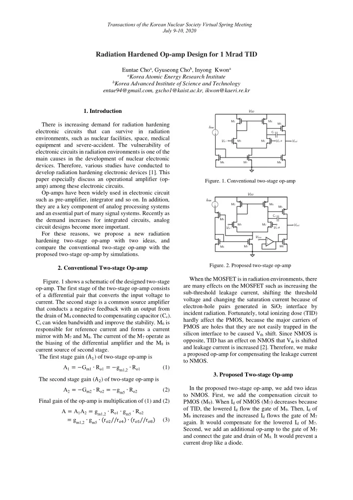
  • Figure. 1 shows a schematic of the designed two-stage
  • p-amp. The first stage of the two-stage op-amp consists
  • f a differential pair that converts the input voltage to
  • current. The second stage is a common source amplifier

that conducts a negative feedback with an output from the drain of M4 connected to compensating capacitor (Cc). Cc can widen bandwidth and improve the stability. M6 is responsible for reference current and forms a current mirror with M7 and M8. The current of the M7 operate as the biasing of the differential amplifier and the M8 is current source of second stage. The first stage gain (A1) of two-stage op-amp is A1 = −Gm1 ∙ Ro1 = −gm1,2 ∙ Ro1 (1) The second stage gain (A2) of two-stage op-amp is A2 = −Gm2 ∙ Ro2 = −gm5 ∙ Ro2 (2) Final gain of the op-amp is multiplication of (1) and (2) A = A1A2 = gm1,2 ∙ Ro1 ∙ gm5 ∙ Ro2 = gm1,2 ∙ gm5 ∙ (r𝑝2//r𝑝4) ∙ (r𝑝5//r𝑝8) (3)

  • Figure. 1. Conventional two-stage op-amp
  • Figure. 2. Proposed two-stage op-amp

When the MOSFET is in radiation environments, there are many effects on the MOSFET such as increasing the sub-threshold leakage current, shifting the threshold voltage and changing the saturation current because of electron-hole pairs generated in SiO2 interface by incident radiation. Fortunately, total ionizing dose (TID) hardly affect the PMOS, because the major carriers of PMOS are holes that they are not easily trapped in the silicon interface to be caused Vth shift. Since NMOS is

  • pposite, TID has an effect on NMOS that Vth is shifted

and leakage current is increased [2]. Therefore, we make a proposed op-amp for compensating the leakage current to NMOS.

  • 3. Proposed Two-stage Op-amp

In the proposed two-stage op-amp, we add two ideas to NMOS. First, we add the compensation circuit to PMOS (M9). When Id of NMOS (M7) decreases because

  • f TID, the lowered Id flow the gate of M9. Then, Id of

M9 increases and the increased Id flows the gate of M7

  • again. It would compensate for the lowered Id of M7.

Second, we add an additional op-amp to the gate of M7 and connect the gate and drain of M8. It would prevent a current drop like a diode.

slide-2
SLIDE 2

Transactions of the Korean Nuclear Society Virtual Spring Meeting July 9-10, 2020

As shown in Figure. 3, the layout consists of and proposed op-amps using eleven pads. The total chip size is 942.8 μm width and 956.6 μm length.

  • 4. Simulation Results

In order to compare the op-amps in two different environments, pre-radiation and radiation by simulations. The designed op-amp fabricated in 180 nm process

  • perates at the supply voltage of 1.8 V. Vbias of the

proposed op-amp is 0.8 V. Ibias of conventional and proposed op-amps are 54 μA and 84 μA, respectively. 4.1 In Pre-Radiation Specification The conventional op-amp exhibits a gain of 51 dB with a 52° phase margin in pre-radiation environments. After corner simulation, gain value drops to 46 dB when ‘fast/fast’, and it increases to 52 dB when ‘slow/slow’. The proposed op-amp exhibits a gain of 40 dB with a 60° phase margin in pre-radiation environments. After corner simulation, gain value drops to 36.2 dB when ‘fast/fast’, and it increases to 40.3 dB when ‘slow/slow’. 4.2 In Radiation Specification We connect an additional current source modeled by radiation impact events to M2 to simulate irradiation test. We connect only one current source to maximize the experimental results, but it will be actually less impact. After looking at the papers about leakage current, we can derive this equation in common [2], [3]. I𝑚𝑓𝑏𝑙𝑏𝑕𝑓 𝑑𝑣𝑠𝑠𝑓𝑜𝑢 ≅ 𝐵 (

𝑋 𝑀 ) log 𝑈𝐽𝐸 + 𝐶

(4) where A is about 10-8 and B is about 10-9 as the initial leakage current. The (

𝑿 𝑴 ) of M2 is ( 𝟒𝟏 𝟏.𝟐𝟗). The equation

(4) shows that the leakage current flow tens of μA at 1

  • Mrad. So we assume that the leakage current source

induced by radiation effects is 15 μA. Next, we compare the conventional op-amp with the proposed op-amp by simulation. Table. Ⅰ shows each simulation result. The conventional op-amp comes out the 28 dB gain with the 61° phase margin after irradiation. By contrast, the proposed op-amp comes out the 36 dB gain with the 62° phase margin after irradiation. Compared to before irradiation, the gain of conventional

  • p-amp drops 45% from 51 dB to 28 dB and the gain of

proposed op-amp drops 10% from 40 dB to 36 dB. Figure. 4 shows the gain value versus the calculated irradiation dose of the conventional op-amp and the proposed op-

  • amp. This shows that the proposed op-amp is highly

stable in the radiation environments.

  • 5. Conclusion

We design the radiation hardened two-stage op-amp that compensate the leakage current using an internal op- amp when the current drop in radiation environments. The simulation results show that gain drop of conventional and proposed op-amps are 45% and 10% for 1 Mrad, respectively. It verifies that the proposed op- amp compensates for leakage current better than conventional op-amp, like the theoretical predictions. After the chip is completed, we will perform irradiation tests. The irradiation tests will actually show that the proposed op-amp can withstand high radiation better than the conventional op-amp in radiation environments.

Before irradiation 1 Mrad irradiation Conventional

  • p-amp

Proposed

  • p-amp

Conventional

  • p-amp

Proposed

  • p-amp

Gain (dB) 51 40 28 (45 %) 36 (10 %) Phase Margin (deg) 52 60 61 62 Gain Band Width (MHz) 76 97 41 83 3dB Band Width (MHz) 0.19 1.05 1.4 1.7

  • Table. I. Simulation results of two-stage op-amp
  • Figure. 4. Gain versus calculated irradiation dose of

conventional and proposed op-amps

  • Figure. 3. Layout included conventional and proposed op-amps
slide-3
SLIDE 3

Transactions of the Korean Nuclear Society Virtual Spring Meeting July 9-10, 2020

Acknowledgements This work was supported in part by Basic Science Research Program through the National Research Foundation of Korea (NRF) funded by the Ministry of Science and ICT (2017M2A8A4017932 and 2020M2A8A1000830). References

[1] P.W. Nicholson, Nuclear Electronics, John Wiley & Sons, Inc., London, UK, 1974, pp. 44-118. [2] S. İlik, A. Kabaoğlu, N. Şahin Solmaz and M. B. Yelten, "Modeling of Total Ionizing Dose Degradation on 180-nm n- MOSFETs Using BSIM3," in IEEE Transactions on Electron Devices, vol. 66, no. 11, pp. 4617-4622, Nov. 2019. [3] Minwoong Lee, Seongik Cho, Namho Lee, Jongyeol Kim, Radiation-tolerance analysis of I-gate n-MOSFET according to isolation oxide module in the CMOS bulk process, Microelectronic Engineering, Volume 200, 2018, Pages 45-50