
SLIDE 1
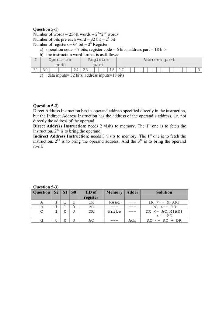
Question 5-1) Number of words = 256K words = 28*210 words Number of bits pre each word = 32 bit = 25 bit Number of registers = 64 bit = 26 Register a) operation code = 7 bits, register code = 6 bits, address part = 18 bits b) the instruction word format is as follows: I Operation code Register part Address part 31 30 24 23 18 17 0 c) data inputs= 32 bits, address inputs=18 bits Question 5-2) Direct Address Instruction has its operand address specified directly in the instruction, but the Indirect Address Instruction has the address of the operand’s address, i.e. not directly the address of the operand. Direct Address Instruction: needs 2 visits to memory. The 1st one is to fetch the instruction, 2nd is to bring the operand. Indirect Address Instruction: needs 3 visits to memory. The 1st one is to fetch the instruction, 2nd is to bring the operand address. And the 3rd is to bring the operand itself. Question 5-3) Question S2 S1 S0 LD of register Memory Adder Solution A 1 1 1 IR Read
- IR <-- M[AR]
B 1 1 0 PC
- PC <-- TR
C 1 0 0 DR Write
- DR <- AC,M[AR]
<-- AC d 0 0 0 AC
- Add