SLIDE 1
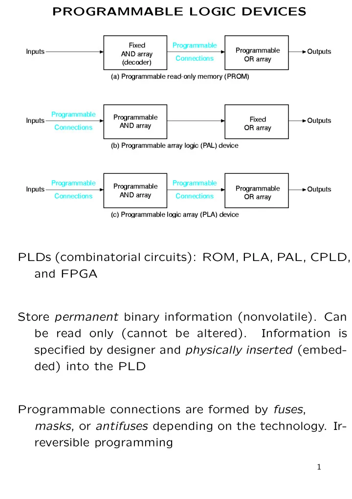
PROGRAMMABLE LOGIC DEVICES PLDs (combinatorial circuits): ROM, PLA, PAL, CPLD, and FPGA Store permanent binary information (nonvolatile). Can be read only (cannot be altered). Information is specified by designer and physically inserted (embed- ded) into the PLD Programmable connections are formed by fuses, masks, or antifuses depending on the technology. Ir- reversible programming
1
SLIDE 2 Read-Only Memory k inputs (address) ⇒ 2k × n ROM ⇒ n outputs (data) 32 × 8 ROM
- k × 2k decoder to decode input address
- n OR gates with 2k input each
- Decoder output is connected to all n OR gates
through fuses
- ROM → 2k × n programmable connections
2
SLIDE 3 Programming a ROM Example of 4 × 2 ROM Truth table Address Content I1 I0 A1 A0 1 1 1 1 1 1 1 1 1 NonProgrammed ROM
2−to−4 Decoder I0 I1 A1 A0 D0 D1 D2 D3
⇓ Programmed ROM
2−to−4 Decoder I0 I1 A1 A0 D0 D1 D2 D3
Compact ROM
A1 A0 2−to−4 Decoder I0 I1 D0 D1 D2 D3
Truth table → address and content of ROM Programming → stores truth table in ROM
- 0 = Open connection = Fuse blown
- 1 = Closed connection = Fuse intact
3
SLIDE 4
Function Synthesis with ROM Any set of functions f1(xk, . . . , x1), . . ., fn(xk, . . . , x1) can be realized with a 2k × n ROM Example: Implement f1(x2, x1) = m(0, 3), f2(x2, x1) = x2 + x1, and f3(x2, x1) = M(1) with a 4 × 3 ROM Truth table Address Content x2 x1 f3 f2 f1 1 1 1 1 1 1 1 1 1 1 ⇓ 4 × 3 ROM storing f1, f2, f3
2−to−4 Decoder D0 D1 D2 D3 f3 f1 f2 x1 x2
4
SLIDE 5 Programmable Logic Array
k AND gates m OR gates n inputs m outputs n x k fuses m fuses n inverters m inverters k x m fuses
Behave like a ROM but has different structure
- Uses ANDs array instead of decoder to produce
product terms of inputs
- Has programmable connections before ANDs, be-
tween ANDs and ORs, after ORs. That is 2nk + km + m fuses
- More flexible than ROM but more difficult to pro-
gram
- Logic expressions for content information to be
stored in PLA must be obtained fisrt, then mini- mized, and finally programmed into the PLA using a PLA program table
- PLA program table specifies product terms and
sum terms of information that will be stored in PLA
5
SLIDE 6
Programming a PLA PLA Program Table Inputs Outputs Term Term# A B C F1 F2 A ¯ B 1 1 1 AC 2 1 1 1 1 BC 3 1 1 1 ¯ AB ¯ C 4 1 1 T C Corresponding PLA Implementation
6
SLIDE 7
Function Synthesis with PLA Any set of functions f1(x1, . . . , xn), . . ., fm(x1, . . . , xn) can be realized with a PLA Example Implement f1(a, b, c) = m(3, 5, 6, 7) and f2(a, b, c) = m(0, 2, 4) with a PLA First Simplify f1, ¯ f1, f2, ¯ f2, that is f1(a, b, c) = ab + ac + bc ¯ f1(a, b, c) = ¯ a¯ b + ¯ a¯ c + ¯ b¯ c f2(a, b, c) = ¯ a¯ c + ¯ b¯ c ¯ f2(a, b, c) = ab + c f1, f2 → 5 terms f1, ¯ f2 → 4 terms ¯ f1, f2 → 3 terms ¯ f1, ¯ f2 → 5 terms Second Select combination of functions that has less terms, that is f1 = ¯ f1 = ¯ a¯ b + ¯ a¯ c + ¯ b¯ c f2(a, b, c) = ¯ a¯ c + ¯ b¯ c Third Construct a PLA program table from selected functions Inputs Outputs Term Term# a b c f1 f2 ¯ a¯ b 1 1 ¯ a¯ c 2 1 1 ¯ b¯ c 3 1 1 C T
7
SLIDE 8
Function Synthesis with PLA (continued) Third Construct a PLA program table from selected functions Inputs Outputs Term Term# a b c f1 f2 ¯ a¯ b 1 1 ¯ a¯ c 2 1 1 ¯ b¯ c 3 1 1 C T Fourth Construct PLA circuit from PLA program table
8
SLIDE 9 Programmable Array Logic
n x k fuses n inverters k AND gates m OR gates n inputs m outputs
Similar to PLA
- Only the connection inputs to ANDs are
programmable
- Easier to program than but not as flexible as PLA
- There are feedback connections
- Logic expressions for content information to be
stored in PAL must be obtained fisrt, then mini- mized, and finally programmed into the PAL using a PAL program table
- PAL program table specifies only product terms
- f information that will be stored in PAL
9
SLIDE 10
Programming a PAL
10
SLIDE 11 Arithmetic-Logic Unit Essential element of the Central Processing Unit Arithmetic and logic functions on binary words
- n-bit data inputs A and B
- n-bit data output G = f(A, B)
- Selection inputs S0, S1 select a function f
- Selection input S2 select an operating mode (arith-
metic or logic)
11
SLIDE 12
ALU (continued) Logic Circuit Arithmetic Circuit
12
SLIDE 13
ALU (continued) 4-bit Arithmetic Circuit
13
SLIDE 14
ALU (continued) Arithmetic and Logic Circuit
14