SLIDE 1
Special Topics in Optical Engineering II (15/1) Minkyu Kim
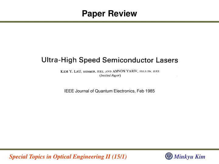
Paper Review
IEEE Journal of Quantum Electronics, Feb 1985
SLIDE 2
Special Topics in Optical Engineering II (15/1) Minkyu Kim
Contents
Semiconductor laser review High speed semiconductor laser Parasitic elements limitations Intermodulation products Intensity noise Large signal effects Conclusion
SLIDE 3 Special Topics in Optical Engineering II (15/1) Minkyu Kim
Interaction between light and matters
+
<Photon interacting with an hydrogen atom> Three interaction processes are possible Absorption Spontaneous Emission Stimulated Emission
𝑆12 = 𝐶12 ∙ 𝑂1 ∙ 𝜍 𝑆𝑡𝑞 = 𝐶𝑡𝑞 ∙ 𝑂2 𝑆21 = 𝐶21 ∙ 𝑂2 ∙ 𝜍
𝜍 : photon density, 𝑂1,2: electron density at 𝐹1,2 𝐶12,21,𝑡𝑞: constants
SLIDE 4 Special Topics in Optical Engineering II (15/1) Minkyu Kim
Interaction between light and matters
Absorption Spontaneous Emission Stimulated Emission
𝑆12 = 𝐶12 ∙ 𝑂1 ∙ 𝜍 𝑆𝑡𝑞 = 𝐶𝑡𝑞 ∙ 𝑂2 𝑆21 = 𝐶21 ∙ 𝑂2 ∙ 𝜍
𝜍 : photon density, 𝑂1,2: electron density at 𝐹1,2 𝐶12,21,𝑡𝑞: constants
𝑆12 = 𝑆𝑡𝑞 + 𝑆21 : Equilibrium condition
𝑂2 𝑂1 = exp − 𝐹2−𝐹1 𝑙𝑈
: Statistical mechanics 𝜍 ℎ𝜉 =
8𝜌ℎ𝜉3 𝑑3{exp ℎ𝜉
𝑙𝑈 −1} : Black-body radiation
𝐶21 𝐶12 = 1, 𝐶𝑡𝑞 𝐶12 = 8𝜌ℎ𝜉3 𝑑3
SLIDE 5
Special Topics in Optical Engineering II (15/1) Minkyu Kim
Optical amplifier
Amplifier
𝑄𝑗𝑜 𝑄𝑝𝑣𝑢 = 𝐻 ∙ 𝑄𝑗𝑜
Stimulated emission should be dominant Pumping 𝑂2 > 𝑂1(Population Inversion)
SLIDE 6 Special Topics in Optical Engineering II (15/1) Minkyu Kim
LASER
LASER : Light Amplification by Stimulated Emission of Radiation LASER = Optical amplifier + Mirrors
- Use initial photon produced by spontaneous emission
- Recycle photons produced by stimulated emission
- Use mirrors for recycling photons
- Condition for sustaining photons in laser
⑴𝑓𝑀 =
1 𝑆 (Gain > mirror loss)
⑵𝑓−𝑘2𝑜𝑙0𝑀 = 1 (No loss after one round trip)
SLIDE 7 Special Topics in Optical Engineering II (15/1) Minkyu Kim
Conditions for lasing
Lasing conditions : ⑴𝑓𝑀 =
1 𝑆 𝑢ℎ = 1 L ln 1 𝑆
⑵𝑓−𝑘2𝑜𝑙0𝑀 = 1𝜇
𝑜 = 2𝑀 𝑛 (𝑛 = 1,2,3, … )
SLIDE 8 Special Topics in Optical Engineering II (15/1) Minkyu Kim
Semiconductor laser
Absorption Spontaneous Emission Stimulated Emission
𝑆12 ℎ𝜉 = 𝐶12 ∙ 𝑂1(𝐹1) ∙ 𝑄2(𝐹2) ∙ 𝜍(ℎ𝜉) 𝑆𝑡𝑞 ℎ𝜉 = 𝐶𝑡𝑞 ∙ 𝑂2(𝐹2) ∙ 𝑄
1(𝐹1)
𝑆21 ℎ𝜉 = 𝐶21 ∙ 𝑂2(𝐹2) ∙ 𝑄
1(𝐹1) ∙ 𝜍(ℎ𝜉)
For population inversion,
𝑂2∙𝑄1 𝑂1∙𝑄2 > 1 Electron & hole should be injected
(Forward bias in PN junction)
SLIDE 9
Special Topics in Optical Engineering II (15/1) Minkyu Kim
Semiconductor laser structure
SLIDE 10 Special Topics in Optical Engineering II (15/1) Minkyu Kim
High speed semiconductor laser
⑴
𝑒𝑂 𝑒𝑢 = 𝐾 𝑓𝑒 − 𝑂 𝜐𝑡 − 𝐵 𝑂 − 𝑂𝑝𝑛 𝑄
⑵
𝑒𝑄 𝑒𝑢 = 𝐵 𝑂 − 𝑂𝑝𝑛 𝑄 − 𝑄 𝜐𝑞 + 𝛾 𝑂 𝜐𝑡
𝑂: carrier density 𝑂𝑝𝑛: carrier density for transparency 𝑄: photon density 𝐾: pump current density 𝑒: thickness of active layer 𝜐𝑡: spontaneous recombination lifetime of carriers 𝜐𝑞: photon lifetime 𝐵: optical gain coefficient 𝛾: fraction of spontaneous emission entering to lasing mode
Rate equations
Small signal & linearization 𝑔
𝑈 𝑠𝑓𝑚𝑏𝑦𝑏𝑢𝑗𝑝𝑜 𝑝𝑡𝑑𝑗𝑚𝑚𝑏𝑢𝑗𝑝𝑜 𝑔𝑠𝑓𝑟𝑣𝑓𝑜𝑑𝑧 = 1
2𝜌 𝐵𝑞0 𝜐𝑞
𝐁 ↑, 𝐪𝟏 ↑, 𝛖𝐪 ↓ high speed semiconductor laser
SLIDE 11 Special Topics in Optical Engineering II (15/1) Minkyu Kim
Parasitic elements limitation
Substrate
n doped confining layer p doped confining layer active layer
𝐽 𝐽
Circuit modeling Semiconductor laser 𝜃 = 𝑑𝑣𝑠𝑠𝑓𝑜𝑢 𝑔𝑚𝑝𝑥𝑗𝑜 𝑗𝑜𝑢𝑝 𝑢ℎ𝑓 𝑗𝑜𝑢𝑠𝑗𝑜𝑡𝑗𝑑 𝑒𝑗𝑝𝑒𝑓 𝑤𝑝𝑚𝑢𝑏𝑓 𝑝𝑔 𝑢ℎ𝑓 𝑡𝑗𝑜𝑏𝑚 𝑡𝑝𝑣𝑠𝑑𝑓 = 1 𝑡2 𝜕0
2 +
𝑡 𝜕0𝑅 + 1 𝜕0 = 50 + 𝑆 𝑀𝑆𝐷 , 𝑅 = 𝑀𝑆𝐷(50 + 𝑆) 𝑀 + 50𝑆𝐷 Second-order low pass filter type
Intrinsic diode Contact resistance Parasitic capacitance Bonding wire
SLIDE 12
Special Topics in Optical Engineering II (15/1) Minkyu Kim
Parasitic elements limitation
SLIDE 13 Special Topics in Optical Engineering II (15/1) Minkyu Kim
Parasitic elements limitation
Circuit modeling 𝑎 = 𝑎0
1+𝑓−2𝑙𝑋 1−𝑓−2𝑙𝑋, W : width of top contact
𝑎0 = 𝑆𝑒𝑗𝑡𝑢 𝑘𝜕𝐷𝑒𝑗𝑡𝑢 , 𝑙 = 𝑘𝜕𝑆𝑒𝑗𝑡𝑢𝐷𝑒𝑗𝑡𝑢 Higher frequency higher propagation constant(k) electric field cannot penetrate far beyond laser junction
SLIDE 14
Special Topics in Optical Engineering II (15/1) Minkyu Kim
Intermodulation products
Third order intermodulation can be a problem in multichannel frequency division transmission Third order intermodulation
SLIDE 15 Special Topics in Optical Engineering II (15/1) Minkyu Kim
Intensity noise
𝑆𝑓𝑚𝑏𝑢𝑗𝑤𝑓 𝐽𝑜𝑢𝑓𝑜𝑡𝑗𝑢𝑧 𝑂𝑝𝑗𝑡𝑓 𝑆𝐽𝑂 = < Δ𝑄 >2 < 𝑄0 >2
𝑄0: average light output power < Δ𝑄 >2: mean square intensity fluctuation spectral density of the light output
With rate equations, 𝑆𝐽𝑂 ~
1 𝑞0 𝜕3
𝜕2 𝜕𝑆 2−1 2
+ 𝜕2
𝜕𝑆 4 𝜐𝑆 2
SLIDE 16
Special Topics in Optical Engineering II (15/1) Minkyu Kim
Large signal effects
Non-linearity problem for large signal
<Effects of increasing optical modulation depth>
Optical modulation depth for high speed below ~70 percent
SLIDE 17 Special Topics in Optical Engineering II (15/1) Minkyu Kim
Conclusion
𝑔
𝑈 = 1
2𝜌 𝐵𝑞0 𝜐𝑞
A ↑, p0 ↑, τp ↓ high speed semiconductor laser
- Parasitic elements limitations
- Intermodulation products
- Intensity noise
- Large signal effects
⑴
𝑒𝑂 𝑒𝑢 = 𝐾 𝑓𝑒 − 𝑂 𝜐𝑡 − 𝐵 𝑂 − 𝑂𝑝𝑛 𝑄
⑵
𝑒𝑄 𝑒𝑢 = 𝐵 𝑂 − 𝑂𝑝𝑛 𝑄 − 𝑄 𝜐𝑞 + 𝛾 𝑂 𝜐𝑡
𝑂: carrier density 𝑂𝑝𝑛: carrier density for transparency 𝑄: photon density 𝐾: pump current density 𝑒: thickness of active layer 𝜐𝑡: spontaneous recombination lifetime of carriers 𝜐𝑞: photon lifetime 𝐵: optical gain coefficient 𝛾: fraction of spontaneous emission entering to lasing mode
Rate equations