SLIDE 1
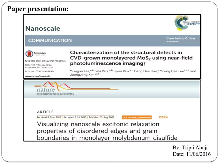
Paper presentation:
By: Tripti Ahuja Date: 11/06/2016
SLIDE 2
SLIDE 3
Background:
MoS2 sheets, a direct band gap semiconducting material has rapid advancement in opto- electronic devices and other processes like photoluminescence (PL) imaging. Using PL property of MoS2 , scanning near field optical microscopy (SNOM) was integrated with PL technique to identify nanosized line defects and GBs on ML-MoS2 sheet with enhanced resolution. Near field optical microscopy provides a non traditional route to explore material properties below the diffraction limit in 2D systems that confines optical excitation and collection without hindering spectral analysis. Scanning tunneling and transmission electron microscopies are able to probe atomic scale electronic properties and structural defects in ML-TMDCs but exhibit limitations for optical investigations of the electronic properties and bound excited states (excitons and trions) of the 2D materials.
SLIDE 4
In this paper…
They have used SNOM PL imaging technique to resolve nanoscale structural defects as small as 20 nm, such as grain boundaries (GBs) or adlayers of CVD grown ML-MoS2, which were not discernible by conventional PL imaging. SNOM PL imaging was correlated with scanning electron microscopy (SEM) to show that PL quenching at the GB sites on ML-MoS2 resulted mainly from actual physical damage at the GBs rather than from the presence of localized states.
From-Witec Manual
SLIDE 5
Method for sample preparation:
CVD grown ML-MoS2 sheet. Substrate here is ITO coated glass or sapphire. 780 °C
http://www.slideshare.net/rahulraghvendra5/mos2-46232395
SLIDE 6 Results and Discussions:
- Fig. 1) SNOM and confocal PL images of butterfly-shaped monolayered MoS2 prepared on an ITO-coated glass substrate.
(a) Confocal PL image and (b) SNOM PL image of monolayered MoS2 on the ITO-coated glass substrate. The gray arrows indicate the expected GB positions. (c) SEM image of the same sample area. The width of a narrow line defect was 20 nm. The scale bar indicates 3 µm. ( a’, b’, and c’) indicate the magnified views of the center area (red box) of each image shown in (a, b, and c). The scale bar in (a’) indicates 1 µm.
SLIDE 7
- Fig. 2) SNOM PL images of polycrystalline monolayered MoS2 flakes. (a) SNOM PL image of a 3-grain merged
- MoS2flake. (b, c) Re-imaged SNOM PL images of the two GB areas (red boxed regions in a). The expected GB position
is indicated in each inset. (d) SNOM PL image of a 4-grain merged MoS2 flake. The inset shows a high-resolution SNOM PL image of the boxed GB area. The white and orange arrows indicate the GB sites. The scale bars in (a, d) indicate 5 µm, and the scale bars in (b, c) and the inset in (d) indicate 1 µm.
SLIDE 8
- Fig. 3) SNOM PL images of monolayered MoS2 flakes with adlayer defects. (a) SNOM PL image of a polycrystalline
monolayered MoS2 flake. Dark triangular adlayer defects were observed on the MoS2 surface. Comparison of (b) confocal PL and (c) SNOM PL images of the same area of the monolayered MoS2. (d) SNOM PL image showing the
- rientations of the adlayer defects. (e) Distribution of the relative orientations of the adlayer defects with respect to
the underlying monolayered MoS2 grain. The scale bars in (a, b, and c) indicate 2 µm, and the scale bar in (d) indicates 1 µm.
SLIDE 9
- Fig. 4) (a) PL-SNOM image to show that freshly cut edge of ML-MoS2 do not show enhanced PL intensity. (b) Plot of
the full width at half maximum (FWHM), as measured in the SNOM PL image vs. the estimated widths measured in the SEM image, of selected line defects. The solid dots represent the actual measured values and the red squares indicate the predicted FWHM values of the line profile obtained by convolution of a Gaussian profile having a 110 nm FWHM and the step function of the corresponding widths measured from the SEM images. The red line provides a guide for the eyes. The insets show the actual SEM and SNOM PL images used to estimate the FWHM.
(b)
SLIDE 10 Conclusions:
Near-field PL images of CVD grown ML-MoS2 were presented to characterize the nanosized line defects and adlayer defects of MoS2. Superb capability of optical PL-SNOM to identify the structural defects of ML-MoS2
PL signal reduction at the GBs across the centered GB line is not always necessarily true.
SLIDE 11
Visualizing nanoscale excitonic relaxation properties of disordered edges and grain boundaries in monolayer molybdenum disulfide
Wei Bao, Nicholas J. Borys, Changhyun Ko, Joonki Suh, Wen Fan, Andrew Thron, Yingjie Zhang, Alexander Buyanin, Jie Zhang, Stefano Cabrini, Paul D. Ashby, Alexander Weber-Bargioni, Sefaattin Tongay, Shaul Aloni, D. Frank Ogletree, Junqiao Wu, Miquel B. Salmeron & P. James Schuck Molecular Foundry, Lawrence Berkeley National Laboratory, USA
Published: 13 Aug 2015 DOI: 10.1038/ncomms8993
SLIDE 12
In this paper…
They have utilized their previously established sub-diffraction hyperspectral imaging capability of their campanile probe to spectroscopically map nanoscale excited-state relaxation processes in chemical vapor deposition (CVD) grown ML- MoS2sheet. The enhanced resolution of ML-MoS2 images revealed the significant optoelectronic heterogeneity. These images have also enabled to quantify the exciton-quenching phenomena at GBs.
SLIDE 13 Fig 1: SEM images of the typical campanile probe used for the measurement analysis Fig 2: Schematic drawing of the optical beam path used for the near-field hyperspectral
- ptical imaging of ML-MoS2 using campanile probe, (b) A comparison of the spatially
averaged emission spectra collected from the Campanile near field probe and traditional confocal microscopy (100X 0.7 NA objective) for the ML-MoS2 flake.
SLIDE 14 Results and Discussions:
Figure 3: Nano-optical imaging of PL in ML-MoS2. (a) Illustration of near-field excitation and collection of the PL from ML-MoS2 using the Campanile near-field probe where the optical laser excitation (2.33 eV) and collection of sample emission are confined to the apex of the tip to produce high resolution optical maps. At each pixel a full PL spectrum is
- acquired. (b) Map of the PL emission intensity of a triangular ML-MoS2 flake using the Campanile probe. The white dashed
line indicates the flake boundary as determined from the shear-force topography. Scale bar, 1mm. (c) An image of the same flake acquired with scanning confocal microscopy using a 100-X, 0.7-NA air objective. Scale bar, 1mm. (d) Near-field nano- PL spectrum averaged over the spatial extent of the ML-MoS2 flake. The emission contains two peaks arising from the radiative recombination from exciton (A) and trion (A -)states . The dashed vertical line shows the position of the spectral median (SM) that splits the spectrum into equal amounts of high and low energy countsand is used to quantify spectral variations in the lower signal-to-noise spectra of individual spatial positions acquired during fast scans. All data were acquired under ambient conditions. NA, numerical aperture
SLIDE 15
Comparative study of two papers:
Difgerent aspects Nanoscale paper Nature Communications paper Basic study Characterization of nanosized GBs and adlayer defects on ML-MoS2 sheet Visualization of excitonic relaxation phenomena at edges and GBs at nanoscale level Sample preparation method CVD grown ML- MoS2 CVD grown ML-MoS2 T echnique SNOM-PL but aperture cantilever probe is used SNOM utilizing PL property of ML-MoS2 but hyperspectral imaging campanile probe is used Imaging and spectral analysis Only SNOM-PL imaging of ML- MoS2 is done SNOM imaging with spectral analysis is done.
SLIDE 16
SLIDE 17
Future plan:
To study the optical and electronic effects of one layered material on the other layered material in Van der Waals layered heterostructures. Since edge defects and the GBs are important from sense of catalytic activity, one can monitor the catalytic activity of biological molecules like proteins, enzymes etc with the different nanoparticle systems.