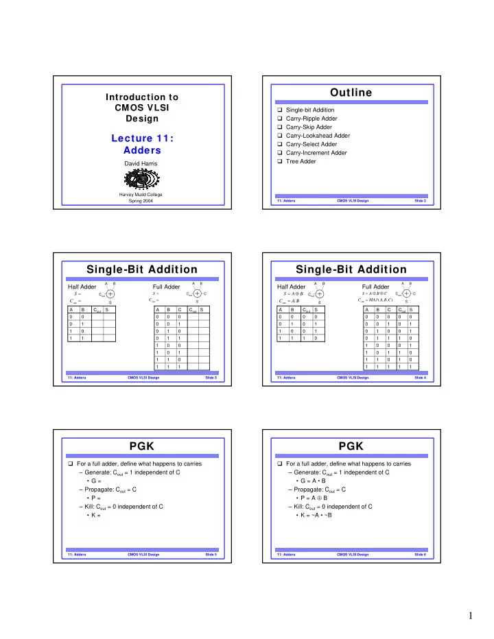
outline
play

Outline Introduction to CMOS VLSI Single-bit Addition Design - PDF document

Outline Introduction to CMOS VLSI Single-bit Addition Design Carry-Ripple Adder Carry-Skip Adder Carry-Lookahead Adder Lecture 11: Carry-Select Adder Adders Carry-Increment Adder Tree Adder David Harris Harvey Mudd


  1. Outline Introduction to CMOS VLSI � Single-bit Addition Design � Carry-Ripple Adder � Carry-Skip Adder � Carry-Lookahead Adder Lecture 11: � Carry-Select Adder Adders � Carry-Increment Adder � Tree Adder David Harris Harvey Mudd College Spring 2004 11: Adders CMOS VLSI Design Slide 2 Single-Bit Addition Single-Bit Addition A B A B A B A B Half Adder Full Adder Half Adder Full Adder = = ⊕ = = ⊕ ⊕ S S S A B S A B C C out C C out C C out C out = = = = C C MAJ A B C ( , , ) C C A B ฀ out S out S S S out out A B C out S A B C C out S A B C out S A B C C out S 0 0 0 0 0 0 0 0 0 0 0 0 0 0 0 1 0 0 1 0 1 0 1 0 0 1 0 1 1 0 0 1 0 1 0 0 1 0 1 0 0 1 1 1 0 1 1 1 1 1 0 0 1 1 1 0 1 0 0 1 0 0 0 1 1 0 1 1 0 1 1 0 1 1 0 1 1 0 1 0 1 1 1 1 1 1 1 1 11: Adders CMOS VLSI Design Slide 3 11: Adders CMOS VLSI Design Slide 4 PGK PGK � For a full adder, define what happens to carries � For a full adder, define what happens to carries – Generate: C out = 1 independent of C – Generate: C out = 1 independent of C • G = • G = A • B – Propagate: C out = C – Propagate: C out = C • P = A ⊕ B • P = – Kill: C out = 0 independent of C – Kill: C out = 0 independent of C • K = • K = ~A • ~B 11: Adders CMOS VLSI Design Slide 5 11: Adders CMOS VLSI Design Slide 6 1

  2. Full Adder Design I Full Adder Design II � Brute force implementation from eqns � Factor S in terms of C out = ⊕ ⊕ S = ABC + (A + B + C)(~C out ) S A B C � Critical path is usually C to C out in ripple adder = C MAJ A B C ( , , ) out MINORITY A A A B B C C B C A A C out S B B S A B B S C C C A B B S A MAJ C out C C C A B C out C B B B C A A B B A A C out 11: Adders CMOS VLSI Design Slide 7 11: Adders CMOS VLSI Design Slide 8 Layout Full Adder Design III � Clever layout circumvents usual line of diffusion � Complementary Pass Transistor Logic (CPL) – Use wide transistors on critical path – Slightly faster, but more area B – Eliminate output inverters B B C B C A B C B C S C out A B C B C A B C B C S C out B A B 11: Adders CMOS VLSI Design Slide 9 11: Adders CMOS VLSI Design Slide 10 Full Adder Design IV Carry Propagate Adders � Dual-rail domino � N-bit adder called CPA – Very fast, but large and power hungry – Each sum bit depends on all previous carries – Used in very fast multipliers – How do we compute all these carries quickly? φ φ C out _h C out _l C_h A_h C_l A_l A N...1 B N...1 A_h B_h B_h A_l B_l B_l C out C out C in C in 00000 11111 carries φ C out C in S_l S_h + A 4...1 1111 1111 C_l C_h C_h +0000 +0000 B 4...1 1111 0000 S 4...1 S N...1 B_l B_h B_h A_h A_l 11: Adders CMOS VLSI Design Slide 11 11: Adders CMOS VLSI Design Slide 12 2

  3. Carry-Ripple Adder Inversions � Simplest design: cascade full adders � Critical path passes through majority gate – Critical path goes from Cin to Cout – Built from minority + inverter – Design full adder to have fast carry delay – Eliminate inverter and use inverting full adder A 4 B 4 A 3 B 3 A 2 B 2 A 1 B 1 A 4 B 4 A 3 B 3 A 2 B 2 A 1 B 1 C out C in C out C in C 3 C 2 C 1 C 3 C 2 C 1 S 4 S 3 S 2 S 1 S 4 S 3 S 2 S 1 11: Adders CMOS VLSI Design Slide 13 11: Adders CMOS VLSI Design Slide 14 Generate / Propagate Generate / Propagate � Equations often factored into G and P � Equations often factored into G and P � Generate and propagate for groups spanning i:j � Generate and propagate for groups spanning i:j = = + ฀ G G G P G − i j : i j : i k : i k : k 1: j = = ฀ P 0:00:0 0 in GC 0:00:0 0 in GC P P P 0:00:0 0 in GC 0:00:0 0 in GC − i j : i j : i k : k 1: j � Base case � Base case ≡ = ≡ = ≡ = G G ≡ = G G C G G G G A ฀ B 0:0 0 0:0 0 in i i : i i i : i i i ≡ = ≡ = ≡ = ≡ = ⊕ P P P P 0 P P P P A B 0:0 0 0:0 0 i i : i i i : i i i � Sum: � Sum: S = = ⊕ S P G − i i i i 1:0 11: Adders CMOS VLSI Design Slide 15 11: Adders CMOS VLSI Design Slide 16 PG Logic Carry-Ripple Revisited = + ฀ A 4 B 4 A 3 B 3 A 2 B 2 A 1 B 1 C in G G P G − i :0 i i i 1:0 A 4 B 4 A 3 B 3 A 2 B 2 A 1 B 1 C in 1: Bitwise PG logic G 4 P 4 G 3 P 3 G 2 P 2 G 1 P 1 G 0 P 0 G 4 P 4 G 3 P 3 G 2 P 2 G 1 P 1 G 0 P 0 2: Group PG logic G 3:0 G 2:0 G 1:0 G 0:0 G 3:0 G 2:0 G 1:0 G 0:0 C 3 C 2 C 1 C 0 3: Sum logic C 3 C 2 C 1 C 0 C 4 C 4 C out S 4 S 3 S 2 S 1 C out S 4 S 3 S 2 S 1 11: Adders CMOS VLSI Design Slide 17 11: Adders CMOS VLSI Design Slide 18 3

  4. Carry-Ripple PG Diagram Carry-Ripple PG Diagram Bit Position Bit Position 15 14 13 12 11 10 9 8 7 6 5 4 3 2 1 0 15 14 13 12 11 10 9 8 7 6 5 4 3 2 1 0 = = + − + t t t ( N 1) t t ripple ripple pg AO xor Delay Delay 15:0 14:0 13:0 12:0 11:0 10:0 9:0 8:0 7:0 6:0 5:0 4:0 3:0 2:0 1:0 0:0 15:0 14:0 13:0 12:0 11:0 10:0 9:0 8:0 7:0 6:0 5:0 4:0 3:0 2:0 1:0 0:0 11: Adders CMOS VLSI Design Slide 19 11: Adders CMOS VLSI Design Slide 20 PG Diagram Notation Carry-Skip Adder � Carry-ripple is slow through all N stages � Carry-skip allows carry to skip over groups of n bits Black cell Gray cell Buffer i:k k-1:j i:k k-1:j i:j – Decision based on n-bit propagate signal A 16:13 B 16:13 A 12:9 B 12:9 A 8:5 B 8:5 A 4:1 B 4:1 i:j i:j i:j P 16:13 P 12:9 P 8:5 P 4:1 1 C 12 1 C 8 1 C 4 1 G i:k G i:k C out C in G i:j G i:j 0 + 0 + 0 + 0 + P i:k P i:k G i:j G i:j G k-1:j G k-1:j S 16:13 S 12:9 S 8:5 S 4:1 P i:j P i:j P i:j P k-1:j 11: Adders CMOS VLSI Design Slide 21 11: Adders CMOS VLSI Design Slide 22 Carry-Skip PG Diagram Carry-Skip PG Diagram 16 15 14 13 12 11 10 9 8 7 6 5 4 3 2 1 0 16 15 14 13 12 11 10 9 8 7 6 5 4 3 2 1 0 16:0 15:0 14:0 13:0 12:0 11:0 10:0 9:0 8:0 7:0 6:0 5:0 4:0 3:0 2:0 1:0 0:0 16:0 15:0 14:0 13:0 12:0 11:0 10:0 9:0 8:0 7:0 6:0 5:0 4:0 3:0 2:0 1:0 0:0 For k n-bit groups (N = nk) For k n-bit groups (N = nk) ( ) = = + ⎡ − + − ⎤ + t t t ⎣ 2 n 1 ( k 1) ⎦ t t skip skip xor pg AO 11: Adders CMOS VLSI Design Slide 23 11: Adders CMOS VLSI Design Slide 24 4

  5. Variable Group Size Carry-Lookahead Adder � Carry-lookahead adder computes G i:0 for many bits 16 15 14 13 12 11 10 9 8 7 6 5 4 3 2 1 0 in parallel. � Uses higher-valency cells with more than two inputs. A 16:13 B 16:13 A 12:9 B 12:9 A 8:5 B 8:5 A 4:1 B 4:1 C out C 12 C 8 C 4 G 16:13 G 12:9 G 8:5 G 4:1 P 16:13 P 12:9 P 8:5 P 4:1 + + + + C in S 16:13 S 12:9 S 8:5 S 4:1 16:0 15:0 14:0 13:0 12:0 11:0 10:0 9:0 8:0 7:0 6:0 5:0 4:0 3:0 2:0 1:0 0:0 Delay grows as O(sqrt(N)) 11: Adders CMOS VLSI Design Slide 25 11: Adders CMOS VLSI Design Slide 26 CLA PG Diagram Higher-Valency Cells 16 15 14 13 12 11 10 9 8 7 6 5 4 3 2 1 0 G i:k G i:j P i:k i:k k-1:l l-1:m m-1:j G k-1:l P k-1:l G l-1:m P l-1:m G m-1:j i:j P i:j P m-1:j 16:0 15:0 14:0 13:0 12:0 11:0 10:0 9:0 8:0 7:0 6:0 5:0 4:0 3:0 2:0 1:0 0:0 11: Adders CMOS VLSI Design Slide 27 11: Adders CMOS VLSI Design Slide 28 Carry-Select Adder Carry-Increment Adder � Trick for critical paths dependent on late input X � Factor initial PG and final XOR out of carry-select – Precompute two possible outputs for X = 0, 1 15 14 13 12 11 10 9 8 7 6 5 4 3 2 1 0 – Select proper output when X arrives 13:12 9:8 5:4 � Carry-select adder precomputes n-bit sums 14:12 10:8 6:4 – For both possible carries into n-bit group 15:12 11:8 7:4 A 16:13 B 16:13 A 12:9 B 12:9 A 8:5 B 8:5 A 4:1 B 4:1 0 0 0 + + + C out C 12 C 8 C 4 15:0 14:0 13:0 12:0 11:0 10:0 9:0 8:0 7:0 6:0 5:0 4:0 3:0 2:0 1:0 0:0 1 1 1 C in + + + + = 1 1 1 0 0 0 t increment S 16:13 S 12:9 S 8:5 S 4:1 11: Adders CMOS VLSI Design Slide 29 11: Adders CMOS VLSI Design Slide 30 5

Download Presentation
Download Policy: The content available on the website is offered to you 'AS IS' for your personal information and use only. It cannot be commercialized, licensed, or distributed on other websites without prior consent from the author. To download a presentation, simply click this link. If you encounter any difficulties during the download process, it's possible that the publisher has removed the file from their server.

Recommend


More recommend