NOVEL DEVICE ARCHITECTURES FOR ENABLING ENERGY HARVESTING, LIGHTING, - - PDF document

novel device architectures for enabling energy harvesting
SMART_READER_LITE
LIVE PREVIEW

NOVEL DEVICE ARCHITECTURES FOR ENABLING ENERGY HARVESTING, LIGHTING, - - PDF document

18 TH INTERNATIONAL CONFERENCE ON COMPOSITE MATERIALS NOVEL DEVICE ARCHITECTURES FOR ENABLING ENERGY HARVESTING, LIGHTING, AND COMMUNICATIONS FUNC- TIONALITIES IN COMPOSITES M. Shtein 1 *, B. OConnor 2 , A. Yadav, 2 K. Pipe 2 , S.E. Morris, 3


slide-1
SLIDE 1

1 Introduction Modern aircraft and other vehicles often rely on carbon-fiber composites for their high strength-to- weight ratio and ability to be formed into a variety

  • f shapes. However, many of the crucial functionali-

ties in aircraft (e.g. communications, power, etc.) are implemented using bulky and failure-prone compo- nents carrying a weight penalty. With increasing emphasis on system-wide energy efficiency and weight reduction, there is an opportunity to create novel architectures of devices and composites that combine energy harvesting, energy storage, commu- nications and load-bearing capabilities into a single

  • composite. Likewise, new methods are needed to

fabricate such devices cost-effectively. Here we de- scribe new fiber-based architectures for solar cells, thermal energy conversion devices, and antennas that potentially facilitate integration with structural

  • composites. Additionally, this talk will describe re-

cent advances in the fabrication of energy conver- sion devices at ambient conditions. 2 Fiber-based device architectures 2.1 Organic solar cells on fibers To date, thin-film solid-state organic solar cells have been demonstrated by some laboratories to exceed 9% power conversion efficiency at 1 Sun illumina-

  • tion. While this efficiency does not exceed that of

the best inorganic-based solar cells, the basic device construction (i.e. 100-200 nm thick organic layers sandwiched between <100 nm thick electrodes) po- tentially lends itself to integration with substrates which possess load-bearing properties (e.g. glass- or carbon-fiber). In our laboratory, we have used ther- mal evaporation to deposit small-molecular organic solar cells onto a variety of substrates, including glass fibers. [1,2] Briefly, initial proof-of-principle OPV cells on fibers consisted of archetypal organic heterojunc- tions sandwiched between two electrodes, one of

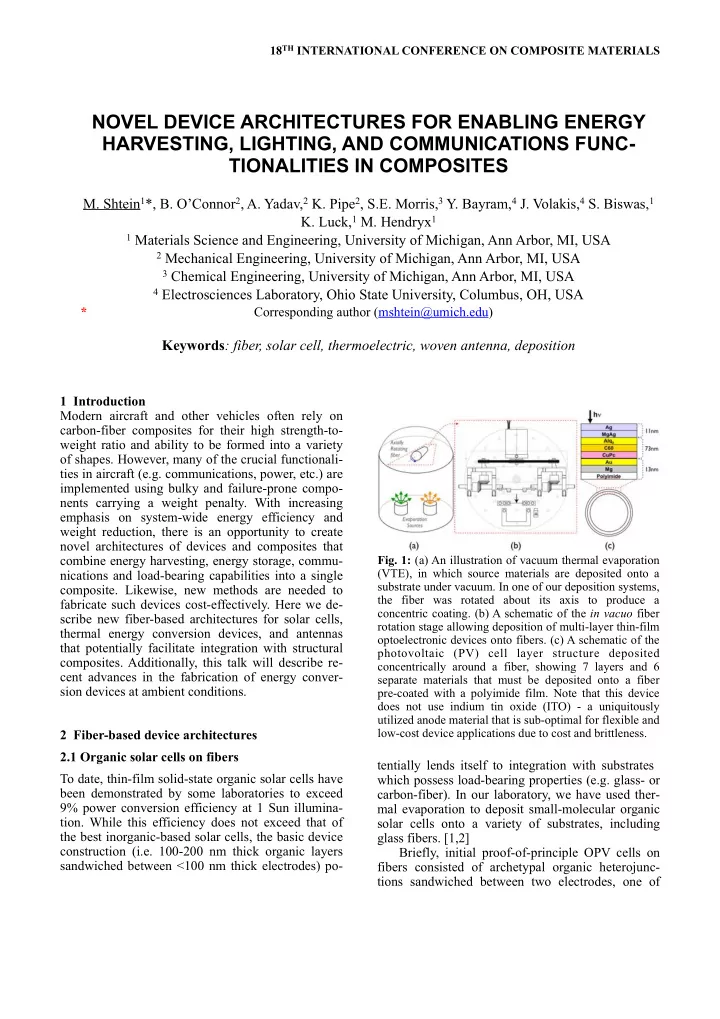
  • Fig. 1: (a) An illustration of vacuum thermal evaporation

(VTE), in which source materials are deposited onto a substrate under vacuum. In one of our deposition systems, the fiber was rotated about its axis to produce a concentric coating. (b) A schematic of the in vacuo fiber rotation stage allowing deposition of multi-layer thin-film

  • ptoelectronic devices onto fibers. (c) A schematic of

the photovoltaic (PV) cell layer structure deposited concentrically around a fiber, showing 7 layers and 6 separate materials that must be deposited onto a fiber pre-coated with a polyimide film. Note that this device does not use indium tin oxide (ITO) - a uniquitously utilized anode material that is sub-optimal for flexible and low-cost device applications due to cost and brittleness.

18TH INTERNATIONAL CONFERENCE ON COMPOSITE MATERIALS

NOVEL DEVICE ARCHITECTURES FOR ENABLING ENERGY HARVESTING, LIGHTING, AND COMMUNICATIONS FUNC- TIONALITIES IN COMPOSITES

  • M. Shtein1*, B. O’Connor2, A. Yadav,2 K. Pipe2, S.E. Morris,3 Y. Bayram,4 J. Volakis,4 S. Biswas,1
  • K. Luck,1 M. Hendryx1

1 Materials Science and Engineering, University of Michigan, Ann Arbor, MI, USA 2 Mechanical Engineering, University of Michigan, Ann Arbor, MI, USA 3 Chemical Engineering, University of Michigan, Ann Arbor, MI, USA 4 Electrosciences Laboratory, Ohio State University, Columbus, OH, USA

* Corresponding author (mshtein@umich.edu)

Keywords: fiber, solar cell, thermoelectric, woven antenna, deposition

slide-2
SLIDE 2

which was transparent. The layer sequence was 25 nm Mg, 20 nm Mg:Au (1:1 by volume), 65 nm Au, 25 nm copper phthalocyanine (CuPc), 40 nm C60, 7 nm tris-(8-hydroxyquinoline) aluminum (Alq3), 6.5 nm Mg:Ag (7:1 by volume), and 5 nm Ag, all depos- ited concentrically onto long fibers that were rotated about their long axis during the deposition process. Control devices consisted of: (a) an identical layer structure deposited onto glass, (b) polyimide foils, and (c) a nearly identical layer structure that omitted the Mg/Mg:Au/Au anode in favor of 100 nm thick indium tin oxide (ITO) anode on glass. The performance parameters of these devices are shown in Table 1. The conventional OPV cell on planar ITO substrates exhibits an efficiency of 1.13%, typical for this set of archetypal materials. Devices replacing the transparent conductor ITO suffer light in-coupling loss, resulting in lower short circuit photocurrent (Jsc), and lower power conver- sion efficiency (ηp). The OPV cells deposited on fi- bers exhibit a lower overall current and voltage than controls on glass and polyimide where light is cou- pled in from the outside, in large part due to the large reflectance of the outer metal electrode at

  • blique incidence angles. Nevertheless, due to the

cylindrical symmetry of the fiber substrate, the fiber- based OPV cells having the same projected are as the planar controls exhibit matching overall power conversion efficiency when perfectly diffuse illumi- nation is considered (i.e. column ηhemi in Table 1). Since this metric considers the more likely scenario

  • f diffuse illumination and mobility of the vehicle
  • n which such a device may be present, we conclude

that the devices having non-planar form factors may have certain advantages, which we explore further with multiple-fiber architectures. Optical and transport simulations of these single-fiber prototype devices were performed and validated by experiment, allow the design in silico of substantially more advanced device geometries, such as bundles of photovoltaic fibers that result in their solar energy harvesting efficiency exceeding that of planar analogues. For example, as described in [3], we explored combinations of multiple fibers, each of which was optimized to (a) increase broadband ab- sorption, and (b) increase absorption within a narrow band of the incident spectrum, complementary to that of other fibers in the bundle, and (c) fibers in configuration (b) but with carefully tuned distributed Bragg reflector coatings surrounding the outer metal

  • electrode. We found that some achievable configura-

tions can exceed 15% power conversion efficiency. Together with the recently calculated fundamental efficiency limits of OPV cells exceeding 20%, [4] these findings further motivate our efforts to scale up the production of fiber-based solar cells, and to integrate them with composites. 2.2 Fiber-based thermoelectric devices Thermoelectric generation of electricity can be ac- complished by connecting two dissimilar materials (metals or semiconductors) in a series of junctions, and sandwiching the junctions between a hot source and a cold sink. The voltage produced by the junc- tion is proportional to the temperature gradient be- tween the hot and cold sides. We can reproduce the conventional series- connected junction geometry in the form of thin-film segments deposited along fibers (see Fig. 3). Weav- ing these fibers can position the junctions as re- quired for power generation. We have realized such devices utilizing thermally evaporated metal junc- tions along flexible glass fibers, and can predict the power density for a weave consisting of junctions of different types of materials. [5] Using metal junc- tions, sparse weaves, and just 10°C temperature gra- dient, a power density of 5 nW/in2 has been achieved, with >5 mW/in2 predicted for denser weaves and semiconductor coatings.

Table 1: Performance parameters for OPV cells deposited

  • n fibers and the planar control devices. (Illumination

intensity is approximately AM1.5.)

  • Fig. 2: Single-fiber, 2-dimensional and 3-dimensional

arrays of fiber-based OPV cells. The latter incorporates fibers with complementary, narrow-band tuned absorption spectra, resulting in improved overall efficiency. Note that since each OPV coating is less than a micrometer thick, each fiber can be thin (e.g. 50 µm in diameter), allowing the overall bundle to be thin. (See ref. [3])

slide-3
SLIDE 3

PAPER TITLE

2.3 Woven, 3-dimensional antennas Continuing the theme of embedding secondary func- tionality into composites via thin film coatings on fibers, we have also realized conformal, light- weight, damage-resistant antennas. Fundamentally, the highest multi-functional performance for such an antenna is achieved when using a substrate with maximum strength-to-weight ratio, while using a coating with the maximum conductivity-to-weight

  • ratio. We have performed an extensive mapping of

materials properties for a variety of fiber types and conductors, arriving at a family of theoretical curves that exhibit a universal behavior, trading off specific strength for conductance, with a reversed S-shaped

  • curve. Our analysis shows that microfilament yarns

(i.e. fibers consisting of thinner strands) offer the greatest strength-to-weight ratio for the core, pro- vided the individual filaments can be coated with conducting films. We have realized such structures using a variety of methods, including electroless plating, weaving the multi-filament conductors for the first time into a 3-dimensional, flexible, stretch- able, broad-band antenna (Fig. 4). [6]

  • Fig. 3: (a) A cross-section of a thermoelectric generator;

cross-plane heat flow generates in-plane electrical

  • current. (b) Illustration of

how structure (a) may be adapted to a woven fiber geometry. (c) A photograph of a thermoelectric fiber produced by depositing metal thermocouple junctions onto a fiber. (Ref. [5])

3 Scale-up of fabrication 3.1 Reel-to-Reel deposition The results on novel device architectures described above encourage an effort into the scale-up of fiber device fabrication using, for instance, continuous, reel-to-reel manufacturing paradigms. To that end, we have constructed a unique apparatus enabling thermal and vapor deposition of organic and inor- ganic materials onto fibers and ribbons. This talk will discuss briefly the design of this apparatus and the characteristics of initial devices it allows to be produced. 3.2 Vapor Deposition In an effort to maximize the efficiency of material utilization during device fabrication, as well as to enable conformal coating of non-planar substrates, we have been developing a number of techniques, including carrier gas-assisted vapor transport and

  • deposition. In these methods, the organic material to

be deposited is first evaporated into a carrier gas stream and subsequently impinged on the substrate at high velocity. This process can be carried out in vacuum, under an inert gas blanket, or in air by sur- rounding the primary jet with a secondary, guard jet, we are able to purge potential contaminants away

  • Fig. 4: (a) sample of encapsulated conductive yarn. (b)

completed flexible, stretchable broadband antenna woven using the conductive Kevlar yarn shown in (a). [Ref. 6]

  • Fig. 5: A process schematic for continuous fabrication of

fiber-based electronic and optoelectronic devices. 3

slide-4
SLIDE 4

from the working area. The latter method, for exam- ple, allowed us to deposit the active layers for en- ergy conversion devices (e.g. light emitting devices [7]) in air, which have exhibited electrolumines- cence efficiencies comparable to devices with or- ganic layer deposited in vacuum. The carrier gas-assisted vapor transport and deposi- tion approaches are now being used to realize

  • rganic-based solar cells and other functional coat-

ings, potentially enabling scalable fabrication of en- ergy conversion devices at dramatically lower costs than with conventional approaches.

  • Fig. 6: (a) An illustration of

a reel-to-reel procedure for coating fibers with organic compounds using carrier gas-assisted vapor transport and deposition. (b) A drawing

  • f the continuous coating apparatus, based on a table-top

version of the vapor deposition apparatus. Computer control and logging of process parameters, such as pressure, flow rate, and source temperature are used to systematically study the influence of macroscopic variables on microstructure evolution that can lead to more efficient photovoltaic and other devices.

References

[1] B. O’Connor, K-H An, Y. Zhao, K. Pipe, M. Shtein. “Fiber shaped organic light emitting device” Ad- vanced Materials 19, 3897 (2007) [2] B. O’Connor, K. Pipe, M. Shtein. “Fiber based organic photovoltaic devices” Appl. Phys. Lett. 92, 193306 (2008) [3] B. O’Connor, D. Nothern, K. Pipe, M. Shtein. “High efficiency, broadband solar cell architectures based on arrays of volumetrically distributed narrowband pho- tovoltaic fibers.” Optics Expr. 18, A432 (2010) [4] N.C. Giebink, et al. (submitted) [5] A. Yadav, K. Pipe, M. Shtein. “Fiber-based thermoe- lectric generator.” Journal of Power Sources 175, 909 (2008) [6] S.E. Morris, Y. Bayram, L. Zhang, Z. Wang, M. Shtein, J.L. Volakis. “High-Strength, Metalized Fibers for Conformal Load Bearing Antenna Applications.” IEEE Trans. on Antennas & Propag. (in press) [7] S. Biswas, K.P. Pipe, M. Shtein. “Solvent-free, direct printing of organic semiconductors in atmosphere.”

  • Appl. Phys. Lett. 96, 263301 (2010)

gX_shteinm_iccm18.pdf