
SLIDE 1
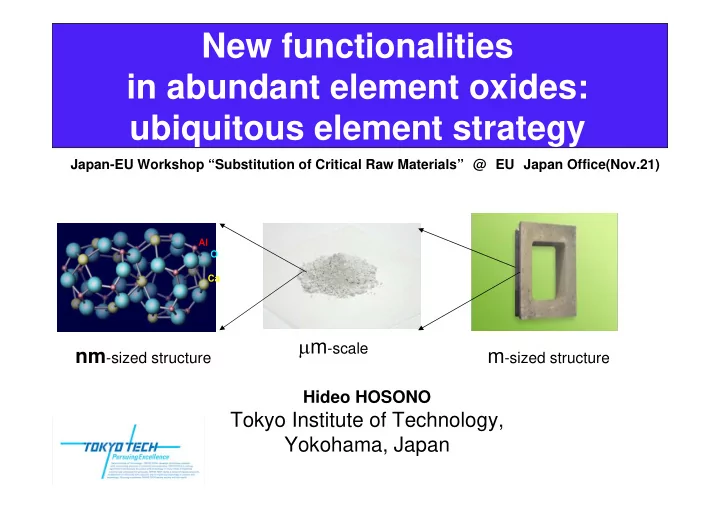
Hideo HOSONO
Tokyo Institute of Technology, Yokohama, Japan
Japan-EU Workshop “Substitution of Critical Raw Materials” @ EU Japan Office(Nov.21)
New functionalities in abundant element oxides: ubiquitous element - - PowerPoint PPT Presentation
New functionalities in abundant element oxides: ubiquitous element strategy Japan-EU Workshop Substitution of Critical Raw Materials @ EU Japan Office(Nov.21) m -scale nm -sized structure m -sized structure Hideo HOSONO Tokyo Institute
Hideo HOSONO
Japan-EU Workshop “Substitution of Critical Raw Materials” @ EU Japan Office(Nov.21)
interface defect nanostructure
Unconventional Valence state
measurement theoretical
Ti 10 H 9 Mg 8 K 7 Na 6 Ca 5 Fe 4 Al 3 Si 2 O 1 Ti 10 H 9 Mg 8 K 7 Na 6 Ca 5 Fe 4 Al 3 Si 2 O 1 Ti 10 H 9 Mg 8 K 7 Na 6 Ca 5 Fe 4 Al 3 Si 2 O 1 Ti 10 H 9 Mg 8 K 7 Na 6 Ca 5 Fe 4 Al 3 Si 2 O 1 Element Order
Clark Number
“Element Strategy for Sustainable society” National Policy (Started from 2008)
size charge
spin
Fe As La
e-
La-O layer Fe-As layer O F Fe As La
e-
La-O layer Fe-As layer O F
Proposal of Transparent Amorphous Oxide Semicoductors (1995) Fabrication of transparent flexible transistor(2004, Nature) 70-inches , UD, 240Hz LCD driven by TAOS-TFT Arrays (Samsung@ FPD Int ’10)
Focusing on Built‐in nanostructure In 12CaO・7Al2O3(1998)
Conversion toTransparet metal. (2004,Science) Breaking a common sense that Iron is the last element for superconductivity
Highest Tc except Cuprates, “2 nd fever”
(2008,JACS & Nature)
High Performance Transistor Transparent metal from Cements
Discovery of a new high Tc
molten metallic electride (2011, Science)
Transparent p-type semiconductor
high precision, high quality ultra low power assumption 2010 2011 2012
tablet computer terminal smart phone
Introduction of IGZO-TFT to Kameyama-2 factory
Production expansion
a-IGZO TFTs are going to apply to iPad3 with high resolution.
JST issued parent license ( non-exclusive) of I GZO-TFT
Unit cell 1.199 nm
Densely Packed Sub-nano-sized Cages
Free Oxygen Ions
Fast Oxygen I on Conductor single crystal powder
2 4 6 Γ Ξ Ρ Ζ Γ Α Μ
Energy (eV)
Ζ
Conduction Band (Framework) Valence Band (Framework) Cage Conduction Band Wave functions confined in cages O2p (Free Oxygen)
PRL(2003), PRB(2005), Nanolett(2007), Adv.Mat (2007)
k
tunneling Evac WF=2.4eV
Adv.Mater. (2007)
Fermi edge
Hard XPS
e–
Out-diffusion of free O2-
[Ca24Al28O64]4+ (2O2–) + Ti → [Ca24Al28O64]4+ (4e–) + TiOX
cage Free O2-
(insulating) (metallic) (Max 2.3x10² 1cm -3)
Science(2003), Nanolett(2007)
Hopping Conduction Band Conduction electron concentration In cages Nc = ~1 × 1021 cm–3 Metal – Insulator Transition
Polaron : electron localized by lattice distortion
Nano Nano Lett
. 2007
3x1019cm -3 2x1021cm -3
JACS.(2007)
100% 100%
Ca Mg Ba Sr Na Li K Rb Cs Al Eu Sm LaB6
Alkaline earth
C12A7:e-
1 2 3 4
Alkaline Rare earth
2.7 2.3 2.2 2.1 2.9
O-LED E-gun
WF=
Li(2.9),Na(2.7),K(2.4), Mg(3.7),Ca(2.9) Adv.Mater(2007) (cage conduction band)
① ② ③ ④ ⑤ ⑥ ① ② ③ ④ ⑤ ⑥
1,2-diol O C Ar H O H H Ar Ar HO OH Al
Encaged electron
Ca
in water
2 4 6 Γ Ξ Ρ Ζ Γ Α Μ
Energy (eV)
Ζ
H -
C12A7:O-
Strong
C12A7:H-
UV(e-beam)-induced Insulator-conductor conversion
C12A7:e-
Field e-emitter Cathode for OLED
3x1019cm -3 2x1021cm -3 3x1019cm -3 2x1021cm -3
MI& MS transition
ReRAM
reagents for organic reaction
C12A7:O2
single cryst. thin film
Low work function but stable
マスク 絶縁性 C12A7:H-
Low work function ~2.4 eV High density of electron trapped cages ~1013/cm2
Low work function electron
Ex Situ I-V characteristics
0.2 ~ 0.3 nm ~ 4 nm ~ 0.2 nm 2 ~ 7 ° atomistic order
1 nm 1 nm 1 nm
Atom density Thermal stability Open mouths : Not observed by experiments Conductivity
ACS Nano (2011)
Solvated cation
Solvated electron
Liquid ammonia
C12A7:O2− Melt C12A7:e− Melt Transparent Strongly Colored
The photo was taken through a color filter
Metallic conducting Ionic conducting Concentration of Solvated electrons ~1021cm-3 Science, 333, 71 (2011)