Multi- scale Manufacturing at Kims Group Things Natural Tunable RF - - PowerPoint PPT Presentation

multi scale manufacturing at kim s group
SMART_READER_LITE
LIVE PREVIEW

Multi- scale Manufacturing at Kims Group Things Natural Tunable RF - - PowerPoint PPT Presentation

Multi- scale Manufacturing at Kims Group Things Natural Tunable RF Energy Nanopipette Photonics 1 cm 10 -2 m Switch Harvesting 10 mm 1,000,000 nanometers = 10 -3 m 1 millimeter (mm) air Microwave substrate 0.1 mm 10 -4 m 100 m


slide-1
SLIDE 1

S.G. KIM, MIT

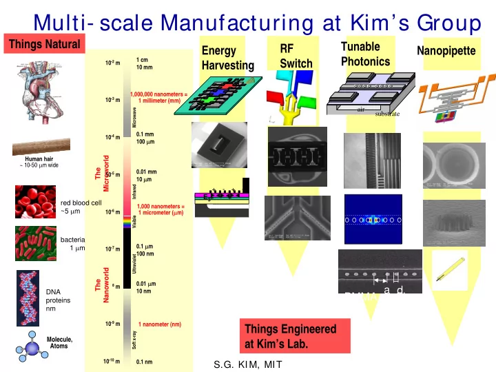
Multi- scale Manufacturing at Kim’s Group

The Microworld

0.1 nm 1 nanometer (nm) 0.01 µm 10 nm 0.1 µm 100 nm 1 micrometer (µm) 0.01 mm 10 µm 0.1 mm 100 µm 1 millimeter (mm) 1 cm 10 mm 10-2 m 10-3 m 10-4 m 10-5 m 10-6 m 10-7 m 10-8 m 10-9 m 10-10 m

Visible

The Nanoworld

1,000 nanometers =

Infrared Ultraviolet Microwave Soft x-ray

1,000,000 nanometers =

DNA proteins nm Molecule, Atoms bacteria 1 µm red blood cell ~5 µm

Human hair ~ 10-50 µm wide

+ - + - + - + E3

Things Natural Energy Harvesting RF Switch Tunable Photonics Nanopipette

air substrate

PMMA on Si a d

Things Engineered at Kim’s Lab.

slide-2
SLIDE 2

Energy Harvesting from Environmental Vibrations

Inter-digitated Electrode PZT ZrO2 + - + - + - + membrane E3

PMPG RF transm itter + Sensor +

Piezoelectric MEMS power generator, d33 mode Monolithic MEMS devices

  • 3V peak, 20 µW/ mm 2
  • Comparable to Li/ LiCoO2 battery

Large-scale Autonomous Wireless Sensor Network

  • Remote sensing of man-made and natural

infrastructures

  • Structural health monitoring (Plants, Planes)
  • Smart bearings for machine diagnostics
  • R. Sood, et al., Hilton Head Conference 2004

S.G. KIM, MIT

slide-3
SLIDE 3

Self- cleaning MEMS switch for 1011 cycles

100 billion cycle direct contact switch

Micro-undulated self-cleaning contact Lateral Au wall by molded electroplating Large strain PZT microactuator

Monolithic MEMS devices

  • Maintain 0.1 Ω for 1 billion cycles and on
  • low insertion loss, high isolation, low voltage

Low cost RF switches

  • GSM cell phones
  • High power military RF switches

Grooved surface Large strain PZT

S.G. KIM, MIT

  • Y. Shi, et al., IEEE MEMS 2005, Miamit, Fl, January

2005

  • N. Conway, et al., IEEE MEMS 2004, Maastricht,

Netherlands, January 2004

slide-4
SLIDE 4

Tunable Photonic Crystals

Electrostatic Actuation1 Piezoelectric Actuation2

Strain tuning of microphotonic devices Monolithic MEMS devices Tunable Gratings1,2 Tunable Microcavity Resonator3 Smart communication devices for all-optical systems

Tunable Photonic Bandgap3

air substrate SiO

2 deformable

membrane integrated tri

  • layer

piezoelectric microactuator 1D photonic crystal microcavity Si waveguide

0.2 0.4 0.6 0.8 1 1430 1470 1510 1550 1590

wavelength (nm) Normalized transmission

band gap band gap

  • 1. Information Sciences, 149, pp. 31-40, 2003

2 . Applied Optics, Vol. 42, No. 4, 2003

  • 3. Appl. Phys. Lett. , V.84,2004

S.G. KIM, MIT

slide-5
SLIDE 5

Transplanting Carbon Nanotubes

Nanostructure assembly, a mechanical way Applications

  • Massive Parallel Nanoprobe

Array

  • Nanopipette
  • Nanotip Cell Manipulation
  • Ultra tough composites

Nanolelleting1

  • Micro-blocks or cylinders with

nanotubes embedded

  • Basic building blocks for

nano-assembly and transplantation

S.G. KIM, MIT

CMPed and Transplanted CNT bundle

1 T. El-Aguizy, et al., Applied Physics Letters, Vol. 85, No. 25, P.5995, 2004

Self-assembly or transplanting nanopellets

slide-6
SLIDE 6

MIT PECVD CNT machine

Required Gas

  • C2H2, CH4, + NH3

Controlled Temp.

  • ver whole substrate (4”φ)
  • 700~ 1200 oC

Working Pressure

  • 1~ 10 Torr

(Base pressure: ~ 10-6 Torr)

  • Temp. measurement

& feedback Large Area Substrate

  • 4” diameter

Plasma Power

  • DC 1000V, 1A

Heated Substrate

S.G. KIM, MIT

slide-7
SLIDE 7

CNT with acetylene gas

S.G. KIM, MIT

slide-8
SLIDE 8

MIT Nanoscanning Platform for Bio Assays

  • Nanotube tip with tunable

stiffness in-plane AFM

  • (Underwater specimen)
  • Simultaneous Imaging and

Pipetting

  • Multi-energy

probing/channeling

  • Arrayable scanning
  • C. Muller-Falcke, et al., Optics East, Philadelphia, PA, October, 2004

S.G. KIM, MIT