
SLIDE 1
1 Intelligent Epitaxy Technology, Inc.
YCKao.3/1/99.C/S Outlook ‘99
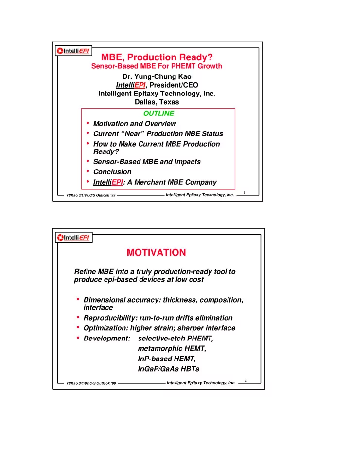
MBE, Production Ready?
Sensor-Based MBE For PHEMT Growth OUTLINE
- Motivation and Overview
- Current “Near” Production MBE Status
- How to Make Current MBE Production
Ready?
- Sensor-Based MBE and Impacts
- Conclusion
- IntelliEPI: A Merchant MBE Company
- Dr. Yung-Chung Kao
IntelliEPI, President/CEO Intelligent Epitaxy Technology, Inc. Dallas, Texas
2 Intelligent Epitaxy Technology, Inc.
YCKao.3/1/99.C/S Outlook ‘99
MOTIVATION
Refine MBE into a truly production-ready tool to produce epi-based devices at low cost
- Dimensional accuracy: thickness, composition,
interface
- Reproducibility: run-to-run drifts elimination
- Optimization: higher strain; sharper interface
- Development: selective-etch PHEMT,