
1
Memory
RWM NVRWM ROM EPROM E2PROM FLASH Random Access Non-Random Access SRAM DRAM Mask-Programmed Programmable (PROM) FIFO Shift Register CAM LIFO
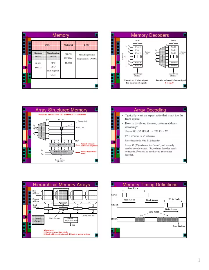
Memory Decoders
Word 0 Word 1 Word 2 Word N-1 Word N-2 Input-Output S0 S1 S2 SN-2 SN_1 (M bits) Storage Cell M bits N Words Word 0 Word 1 Word 2 Word N-1 Word N-2 Input-Output (M bits) Storage Cell M bits Decoder A0 A1 AK-1 S0
N words => N select signals Too many select signals Decoder reduces # of select signals K = log2N
Array-Structured Memory
Input-Output (M bits) Row Decoder AK AK+1 AL-1 2L-K Column Decoder Bit Line Word Line A0 AK-1 Storage Cell Sense Amplifiers / Drivers M.2K
Problem: ASPECT RATIO or HEIGHT >> WIDTH
Amplify swing to rail-to-rail amplitude Selects appropriate word
Array Decoding Hierarchical Memory Arrays
Global Data Bus Row Address Column Address Block Address Block Selector Global Amplifier/Driver I/O Control Circuitry Advantages:
- 1. Shorter wires within blocks
- 2. Block address activates only 1 block => power savings
Memory Timing Definitions
READ WRITE DATA Read Access Read Access Read Cycle Data Valid Data Written Write Access Write Cycle