
SLIDE 1
ECEN5807 Power Electronics 2
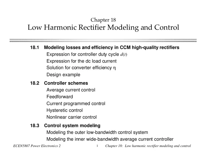
1
Chapter 18: Low harmonic rectifier modeling and control
Low Harmonic Rectifier Modeling and Control 18.1 Modeling losses - - PowerPoint PPT Presentation
Chapter 18 Low Harmonic Rectifier Modeling and Control 18.1 Modeling losses and efficiency in CCM high-quality rectifiers Expression for controller duty cycle d ( t ) Expression for the dc load current Solution for converter efficiency
ECEN5807 Power Electronics 2
1
Chapter 18: Low harmonic rectifier modeling and control
ECEN5807 Power Electronics 2
2
Chapter 18: Low harmonic rectifier modeling and control
+ – Q1 L C R + v(t) – D1 vg(t) ig(t) RL i(t) + – R + v(t) – vg(t) ig(t) RL i(t) DRon + – D' : 1 VF
ECEN5807 Power Electronics 2
3
Chapter 18: Low harmonic rectifier modeling and control
R vac(t) iac(t) + vg(t) – ig(t) + v(t) – id(t) Q1 L C D1 controller i(t) RL
(large)
ECEN5807 Power Electronics 2
4
Chapter 18: Low harmonic rectifier modeling and control
2 4 6 8 10 100 200 300
vg(t) vg(t) ig(t) ig(t)
0° 30° 60° 90° 120° 150° 180°
d(t)
0.2 0.4 0.6 0.8 1 0° 30° 60° 90° 120° 150° 180° 1 2 3 4 5 6
id(t) i(t) = I ωt
0° 30° 60° 90° 120° 150° 180°
ECEN5807 Power Electronics 2
5
Chapter 18: Low harmonic rectifier modeling and control
ECEN5807 Power Electronics 2
6
Chapter 18: Low harmonic rectifier modeling and control
(large)
ECEN5807 Power Electronics 2
7
Chapter 18: Low harmonic rectifier modeling and control
(large)
Tac
2(t)
ECEN5807 Power Electronics 2
8
Chapter 18: Low harmonic rectifier modeling and control
Tac = 2
2
Tac/2
2
Tac/2
ECEN5807 Power Electronics 2
9
Chapter 18: Low harmonic rectifier modeling and control
2
π/2
π/2
ECEN5807 Power Electronics 2
10
Chapter 18: Low harmonic rectifier modeling and control
π/2
ECEN5807 Power Electronics 2
11
Chapter 18: Low harmonic rectifier modeling and control
Tac = V M 2
2
2
ECEN5807 Power Electronics 2
12
Chapter 18: Low harmonic rectifier modeling and control
e
e
ECEN5807 Power Electronics 2
13
Chapter 18: Low harmonic rectifier modeling and control
2
ECEN5807 Power Electronics 2
14
Chapter 18: Low harmonic rectifier modeling and control
e
e
ECEN5807 Power Electronics 2
15
Chapter 18: Low harmonic rectifier modeling and control
ECEN5807 Power Electronics 2
16
Chapter 18: Low harmonic rectifier modeling and control
+ – + –
ECEN5807 Power Electronics 2
17
Chapter 18: Low harmonic rectifier modeling and control
+ – + v(t) – vg(t) ig(t) Gate driver Pulse width modulator Compensator Gc(s)
+ – + –
vref1(t) kx xy x y Multiplier vg(t) vcontrol(t) Gcv(s)
+ –
Voltage reference C vref2(t) v(t) verr(t) va(t)
2
ECEN5807 Power Electronics 2
18
Chapter 18: Low harmonic rectifier modeling and control
+ – + v(t) – vg(t) ig(t) Gate driver Pulse width modulator Compensator Gc(s)
+ – + –
vref1(t) x y multiplier vg(t) vcontrol(t) Gcv(s)
+ –
Voltage reference k v xy z2 z Peak detector VM vref2(t) va(t)
2
ECEN5807 Power Electronics 2
19
Chapter 18: Low harmonic rectifier modeling and control
+ – + v(t) – vg(t) ig(t) Gate driver Pulse width modulator Compensator Gc(s)
+ – + –
vref1(t) x y multiplier vg(t) vcontrol(t) Gcv(s)
+ –
Voltage reference k v xy z2 z Peak detector VM vref2(t) va(t)
2
ECEN5807 Power Electronics 2
20
Chapter 18: Low harmonic rectifier modeling and control
Boost converter Current-programmed controller R vg(t) ig(t) is(t) vg(t) + v(t) – i2(t) Q1 L C D1 vcontrol(t)
Multiplier
X ic(t) = kx vg(t) vcontrol(t) + – + +
+ –
Comparator Latch
ia(t)
Ts
S R Q
ma
Clock
ECEN5807 Power Electronics 2
21
Chapter 18: Low harmonic rectifier modeling and control
Ts =
2(t)fs
2(t)Ts
Ts > TsV
0.2 0.4 0.6 0.8 1 0.0 0.2 0.4 0.6 0.8 1.0
vg(t) V jg(t) = ig(t) Ts Rbase V
CCM DCM Re = Rbase R
e
= 4R
b a s e
Re = . 3 3 Rbase Re = 0.5Rbase Re = 2Rbase Re = 0.2Rbase Re = . 1 Rbase
R
e
= 1 Rb
a s e
ma = V 2L Rbase = 2L Ts
ECEN5807 Power Electronics 2
22
Chapter 18: Low harmonic rectifier modeling and control
Boost converter Wide-bandwidth input current controller vac(t) iac(t) + vg(t) – ig(t) ig(t) vg(t) + vC(t) – i2(t) Q1 L C D1 vcontrol(t)
Multiplier
X +– vref1(t) = kxvg(t)vcontrol(t) Rs va(t) Gc(s) PWM
Compensator
verr(t) DC–DC Converter Load + v(t) – i(t) d(t) +– Compensator and modulator vref3 Wide-bandwidth output voltage controller +– Compensator vref2 Low-bandwidth energy-storage capacitor voltage controller vC(t) v(t)
ECEN5807 Power Electronics 2
23
Chapter 18: Low harmonic rectifier modeling and control
ECEN5807 Power Electronics 2
24
Chapter 18: Low harmonic rectifier modeling and control
ECEN5807 Power Electronics 2
25
Chapter 18: Low harmonic rectifier modeling and control
Re(vcontrol) 〈 vg(t)〉Ts vcontrol + – Ideal rectifier (LFR) ac input dc
+ – 〈 ig(t)〉Ts 〈 p(t)〉Ts 〈 i2(t)〉Ts 〈 v(t)〉Ts C Load
Ts =
Ts 2
2
ECEN5807 Power Electronics 2
26
Chapter 18: Low harmonic rectifier modeling and control
2
2
ECEN5807 Power Electronics 2
27
Chapter 18: Low harmonic rectifier modeling and control
ECEN5807 Power Electronics 2
28
Chapter 18: Low harmonic rectifier modeling and control
2
ECEN5807 Power Electronics 2
29
Chapter 18: Low harmonic rectifier modeling and control
T2L = V + v(t)
T2L = I2 + i2(t)
T2L =
T2L
T2L
2
T2L
T2L, vcontrol(t))
ECEN5807 Power Electronics 2
30
Chapter 18: Low harmonic rectifier modeling and control
vg,rms = Vg,rms
T2L, Vcontrol)
T2L v T2L = V
vcontrol = Vcontrol
2
2(Vcontrol)
vcontrol = Vcontrol
ECEN5807 Power Electronics 2
31
Chapter 18: Low harmonic rectifier modeling and control
ECEN5807 Power Electronics 2
32
Chapter 18: Low harmonic rectifier modeling and control
2
ECEN5807 Power Electronics 2
33
Chapter 18: Low harmonic rectifier modeling and control
vac(t) iac(t) Re + – Ideal rectifier (LFR) C i2(t) ig(t) vg(t) i(t) load + v(t) –
pload(t) = VI = Pload
Energy storage capacitor vC(t) + – Dc-dc converter + – Pload V 〈 pac(t)〉Ts
ECEN5807 Power Electronics 2
34
Chapter 18: Low harmonic rectifier modeling and control
ECEN5807 Power Electronics 2
35
Chapter 18: Low harmonic rectifier modeling and control
+ – + – L C R + 〈v(t)〉Ts – 〈vg(t)〉Ts 〈v1(t)〉Ts 〈i2(t)〉Ts 〈i(t)〉Ts + 〈v2(t)〉Ts – 〈i1(t)〉Ts Averaged switch network
Ts = Vg + vg(t)
Ts = i1(t) Ts = I + i(t)
Ts = v2(t) Ts = V + v(t)
Ts = V1 + v1(t)
Ts = I2 + i2(t)
ECEN5807 Power Electronics 2
36
Chapter 18: Low harmonic rectifier modeling and control
Ts = V + v(t)
Ts
Ts – d'(t)V – d'(t)v(t)
Ts
Ts – d'(t)V – d'(t)v(t)
ECEN5807 Power Electronics 2
37
Chapter 18: Low harmonic rectifier modeling and control
Ts
Ts – d'(t)V – d'(t)v(t)
Ts
Ts – d'(t)V
ECEN5807 Power Electronics 2
38
Chapter 18: Low harmonic rectifier modeling and control
ECEN5807 Power Electronics 2
39
Chapter 18: Low harmonic rectifier modeling and control