learning outcomes
play

Learning Outcomes I understand the PicoBlaze bus interface - PowerPoint PPT Presentation

3-1.1 3-1.2 Learning Outcomes I understand the PicoBlaze bus interface signals: PORT_ID, IN_PORT, OUT_PORT, WRITE_STROBE I understand how a memory map provides the agreement between Spiral 3-1 addresses the software will use and


  1. 3-1.1 3-1.2 Learning Outcomes • I understand the PicoBlaze bus interface signals: PORT_ID, IN_PORT, OUT_PORT, WRITE_STROBE • I understand how a memory map provides the agreement between Spiral 3-1 addresses the software will use and that the hardware must recognize and respond to • I understand how to build address decoding logic to ensure only the appropriate value/register is selected for a given PORTID Hardware/Software Interfacing • For output, I can take a memory map and the PORTID and OUTDATA bits such that the appropriate data is input or saved in a register when an OUTPUT instruction is executed • For input, I can take a memory map and the appropriate PORTID bits to build logic and muxes such that the appropriate data value is present at INDATA when an INPUT instruction is executed 3-1.3 3-1.4 Digital Design Targets • Two possible implementation targets – Custom Chips (ASIC’s = Application Specific Integrated Circuits): Physical gates are created on silicon to implement 1 particular design – FPGA (Field Programmable Gate Array’s): “Programmable logic” using programmable memories to implement logic functions along with other logic resources tiled on the chip. Can implement any design and then be changed to implement a new one 
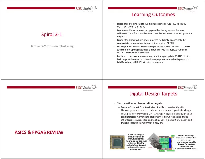
ASICS & FPGAS REVIEW In an ASIC design, a FPGA’s have “logic unique chip will be resources” on them that manufactured that we can configure to implements our design at implement our specific which point the HW design. We can then design is fixed & cannot reconfigure it to be changed (example: implement another design Pentium, etc.)

  2. 3-1.5 3-1.6 ASICs Implementation • ASIC’s – Use the CAD tools to synthesize and route a “netlist” • Synthesis = Takes logic description or logic schematic & converts to transistor level gates • Place and Route = Figure out where each gate should go on the chip) – Final “netlist” is sent to chip maker for production – Fabrication is very expensive (> $1 million) so get your design right the first time. • FPGA’s – Synthesis converts logic description to necessary LUT contents, etc. – Place and route produces a configuration for the FPGA chip – Can reconfigure FPGA as much as you like, so less important to get it right 1 st time 3-1.7 3-1.8 ASIC’s vs. FPGA’s Xilinx Spartan 3E • ASIC’s • FPGA’s Digilent Nexys-2 Board – ___________ – __________________ • Has a Xilinx Spartan 3E FPGA – Handles _______ – ________ Designs (XC3S500e) Designs – ______ Expensive • 500K gate equivalent – _______ Expensive – __________ Flexible • 9312 D-FF’s on-board – _____ Flexible (Cannot On-board I/O be ______________ to perform a new hardware • (4) 7-Segment Displays function) • (8) LED’s • (4) Push Buttons • (8) Switches

  3. 3-1.9 3-1.10 Latest FPGA's • SoC design (Xilinx Kintex [KU115]) – Quad-Core ARM cores – DDR3 SDRAM Memory Interface – ~800 I/O Pins – Equiv. ~15M gate equivalent FPGA fabric Hardware/Software Interfacing • ~1M D-FFs + 552K LUTs PICOBLAZE • 1968 dedicated DSP "slices" 18x18 multiply + adder • 34.6 Megabits of onboard Block RAMs 3-1.11 3-1.12 Input / Output Introduction • Picoblaze (aka KCPSM3) is an 8-bit _____________ • The processor connects to peripherals and other logic – The processor is not implemented directly in hardware on the FPGA via the _______ (address, data, and control) but instead is just a description that is then _______________ using the same process as any of our other designs • Software running on the processor performs _______ – It provides a bus interface that can be connected to custom logic that and _______ that read and write data to and from you design and then used to control that custom logic via __________ these devices based on ________ Processor Memory executing on the processor 0 … 399 A D C Video Interface 800 FE may 254 800 254 signify a WRITE … white dot at 01 a particular location Keyboard Interface 400 61

  4. 3-1.13 3-1.14 Taken from the KCPSM3 Manual Taken from the KCPSM3 Manual 3-1.15 3-1.16 Input / Output Operations Taken from the KCPSM3 Manual Taken from the KCPSM3 Manual

  5. 3-1.17 3-1.18 Exercise 1 Remember: Registers w/ Enables • Registers (D-FF’s) will sample the D • Make the register below capture data bit every clock edge and pass it to Q 1 0 ( out_data ) from your Picoblaze whenever it • Sometimes we may want to hold the SET Y D Q Q value of Q and ignore D even at a D 1 S outputs address FF hex on ( address or CLR clock edge EN CLK • We can add an enable input and port_id ) /AR some logic in front of the D-FF to FF with Data Enable accomplish this OUTDATA CLK /AR EN D i Q i * D[7:0] Q[7:0] Picoblaze INDATA X 0 X X 0 Processor Reg (software 0,1 1 X X Q i ADDR EN controlled) ↑ CLK 1 0 X Q i RST WS (WEN) ↑ 1 1 0 0 ↑ 1 1 1 1 3-1.19 3-1.20 Registers w/ Enables Recall Memory Interfaces • The D value is sampled at the clock edge only • We provide address and 0 1 0 0 0 A[2:0] 1 1 1 1 0 if the enable is active data 2 1 1 0 0 DO[3:0] 3 1 0 1 0 DI[3:0] • Otherwise the current Q value is maintained • EN = Overall enable 4 0 0 1 1 5 0 1 0 0 EN (unless it is 1) the 6 1 0 0 1 WEN 7 0 1 1 0 memory won't read or CLK write (we assume EN=1) CLK • WEN = Write enable CLK /AR A[2:0] 011 110 001 – 1 = Write / 0 = read EN DI[3:0] 1111 D[3:0] WEN 0010 0011 0100 0101 0110 0111 1000 1001 1010 t write M[3] 1010 1111 Q[3:0] 0000 0101 0111 1000 DO[3:0] ??? mem[3] = 1111 mem[6] = 1001 t acc Assume EN=1

  6. 3-1.21 3-1.22 Exercise 1 Exercise 2 • Make the register below capture data • Use your PicoBlaze to receive input from A ( out_data ) from your Picoblaze whenever it given address 00 hex and B for address 0x01 outputs address FF hex on ( address or hex port_id ) OUTDATA 8 OUTDATA D[7:0] Q[7:0] A[7:0] INDATA Picoblaze 8 Picoblaze 0 INDATA Processor Processor Reg B[7:0] 1 (software (software ADDR ADDR EN 8 controlled) controlled) CLK RST WS (WEN) WS (WEN) 3-1.23 3-1.24 Memory Maps Memory Maps • Given an 8-bit address space (256 locations) and 3 devices that we want to interface to our microprocessor, we first must create the memory map • A memory map shows what devices are assigned to a – A 64 bytes (64x8) memory given __________ or address range that can then be – A single 8-bit register accessed by the processor (and its software programs) – A single 1-bit D-FF Dec A7 A6 A5 A4 A3 A2 A1 A0 Assigned Device Dec A7 A6 A5 A4 A3 A2 A1 A0 Assigned Device 00 0 0 0 0 0 0 0 0 64x8 00 0 0 0 0 0 0 0 0 Input Switches 01 0 0 0 0 0 0 0 1 Memory 01 0 0 0 0 0 0 0 1 open … 02 0 0 0 0 0 0 1 0 open 63 0 0 1 1 1 1 1 1 … 64 0 1 0 0 0 0 0 0 8-bit Register 253 1 1 1 1 1 1 0 1 LEDs … open 254 1 1 1 1 1 1 1 0 open 128 1 0 0 0 0 0 0 0 1-bit D-FF 255 1 1 1 1 1 1 1 1 7-Seg Display … open

  7. 3-1.25 3-1.26 Memory Maps Memory Aliasing • Exercise: What is a minimal set of bits that could be used to distinguish • Given each device from the others? – A 64 bytes (64x8) memory => __________ – A 64 bytes (64x8) memory => _______________ – A single 8-bit register => _____________ – A single 8-bit register => _______________ – A single 1-bit D-FF => __________ – A single 1-bit D-FF => __________________ • By using don't care situations the 8-bit register will respond to ____ address where A7-A6 = ___ (i.e. _______) and similarly the 1-bit D-FF will respond to any address where A7=__ (i.e. ___________) Dec A7 A6 A5 A4 A3 A2 A1 A0 Assigned Device Dec A7 A6 A5 A4 A3 A2 A1 A0 Assigned Device 00 0 0 0 0 0 0 0 0 64x8 00 0 0 0 0 0 0 0 0 64x8 01 0 0 0 0 0 0 0 1 Memory 01 0 0 0 0 0 0 0 1 Memory … … 63 0 0 1 1 1 1 1 1 63 0 0 1 1 1 1 1 1 64 0 1 0 0 0 0 0 0 8-bit Register 64 0 1 0 0 0 0 0 0 8-bit Register … open … open 128 1 0 0 0 0 0 0 0 1-bit D-FF 128 1 0 0 0 0 0 0 0 1-bit D-FF … open … open 3-1.27 3-1.28 Address Decoding Memory Maps • Address decoding refers to the process of _____________ the • Exercise: Repeat the exercise to find a minimal set of bits that could be correct device based on a specific address _____________ used to distinguish each device from the others? – A 64 bytes (64x8) memory => ________________________ 64x8 8 8 Memory – A single 8-bit register => ________________________ DI[7:0] DO[7:0] 6 – A single 1-bit D-FF => ____________________________ A[5:0] EN Dec A7 A6 A5 A4 A3 A2 A1 A0 Assigned Device WEN 00 0 0 0 0 0 0 0 0 8-bit Register CLK 0 8 01 0 0 0 0 0 0 0 1 1-bit D-FF 1 Picoblaze 8 Processor 8-bit REG 8 8 02 0 0 0 0 0 0 1 0 64x8 2 (software D[7:0] Q[7:0] 8 3 S1 S0 controlled) 03 0 0 0 0 0 0 1 1 Memory EN WS (WEN) 04 0 0 0 0 0 1 0 0 CLK RST … 64 0 1 0 0 0 0 0 0 0 SET 65 0 1 0 0 0 0 0 1 D Q 1-bit EN DFF 66 0 1 0 0 0 0 1 0 open CLR … open

Download Presentation
Download Policy: The content available on the website is offered to you 'AS IS' for your personal information and use only. It cannot be commercialized, licensed, or distributed on other websites without prior consent from the author. To download a presentation, simply click this link. If you encounter any difficulties during the download process, it's possible that the publisher has removed the file from their server.

Recommend


More recommend