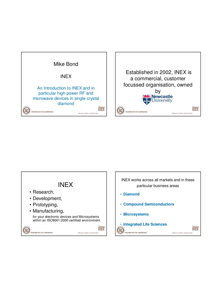
INEX particular business areas Research, Diamond Development, - - PDF document

inex
SMART_READER_LITE
LIVE PREVIEW

INEX particular business areas Research, Diamond Development, - - PDF document

Mike Bond Established in 2002, INEX is INEX a commercial, customer focussed organisation, owned An Introduction to INEX and in by particular high power RF and microwave devices in single crystal diamond PROPRIETARY-IN-CONFIDENCE


slide-1
SLIDE 1

Mike Bond

INEX

An Introduction to INEX and in particular high power RF and microwave devices in single crystal diamond

PROPRIETARY-IN-CONFIDENCE

Established in 2002, INEX is a commercial, customer focussed organisation, owned by

PROPRIETARY-IN-CONFIDENCE

INEX

  • Research,
  • Development,
  • Prototyping,
  • Manufacturing,

for your electronic devices and Microsystems within an ISO9001:2000 certified environment.

PROPRIETARY-IN-CONFIDENCE

INEX works across all markets and in these particular business areas

  • Diamond
  • Compound Semiconductors
  • Microsystems
  • Integrated Life Sciences

PROPRIETARY-IN-CONFIDENCE

slide-2
SLIDE 2

Facilities

  • 400m2 class 100 cleanroom
  • 150 m2 of class 10,000 cleanroom

with local class 100 hoods

  • Toolset based on 150mm

platform (for microsystems development & production)

  • Class 2 cell and molecular biology

laboratories

PROPRIETARY-IN-CONFIDENCE PROPRIETARY-IN-CONFIDENCE

Funded Examples

PROPRIETARY-IN-CONFIDENCE

INEX, owned by Newcastle University, can provide an important role within Regional, National and Internationally Funded projects.

PROPRIETARY-IN-CONFIDENCE

slide-3
SLIDE 3

ReNaChip Rehabilitation of a discrete sensory motor learning function by a prosthetic chip EC Framework 6 Integrated Project: Healthy Aims 26M project involving partners across 9 European countries Develop next generation of implantable medical devices

Commercial Examples

PROPRIETARY-IN-CONFIDENCE

Dual Polarisation Interferometer

– Development of improved waveguide manufacturing process at INEX – Now in production at INEX

PROPRIETARY-IN-CONFIDENCE

slide-4
SLIDE 4

Dual Polarisation Interferometer

“INEX provide production planar waveguides for the world’s first Dual Polarisation Interferometer analytical instrument.”

Press release 2009

PROPRIETARY-IN-CONFIDENCE

Ion mobility spectrometer

–Transferred from Cambridge University as research device –High aspect ratio through-wafer etch –Development and production performed at INEX

PROPRIETARY-IN-CONFIDENCE

Medical parameter measurement device

– INEX developed production prototypes for clinical testing – Now transferring to volume production in 200mm foundry off-shore

PROPRIETARY-IN-CONFIDENCE

Compound Semiconductors

  • InP pHEMT and associated

passives

  • GaN device processing
  • GaAs device processing

– Manufactured GaAs Hall Sensors in the region of 80,000 devices per week – Very high yields

PROPRIETARY-IN-CONFIDENCE

slide-5
SLIDE 5

Diamond

PROPRIETARY-IN-CONFIDENCE

The exploitation of diamond has become possible because

  • f breakthroughs in diamond

synthesis technology, specifically chemical vapour deposition, CVD, that has enabled single crystal diamond to be manufactured with the high purity and consistency required.

Diamond

Diamond as an electrochemical and biological material.

Diamond is a bio-inert and biocompatible material and is ideal for the fabrication of in vivo sensors and electrodes. INEX are active in this field

PROPRIETARY-IN-CONFIDENCE

Diamond

Diamond as an optical material.

Diamond is transparent from the X-ray through the visible and infrared regions of the electromagnetic spectrum. This property combined with high strength and thermal shock make it ideal for X-ray monitors. INEX is active in this field

PROPRIETARY-IN-CONFIDENCE

Diamond

Diamond as an electronic material.

Diamond is a wide bandgap semiconductor and has excellent intrinsic electronic properties especially for high power and frequency applications. For extreme demand applications, single crystal diamond devices are superior to other materials including silicon and gallium arsenide

PROPRIETARY-IN-CONFIDENCE

slide-6
SLIDE 6

Diamond

Very high power RF & microwave devices in single crystal diamond “Largest diamond electronics development activity in the world” (DMD - backed by de Beers through e6 Ltd)

PROPRIETARY-IN-CONFIDENCE

Diamond

Very high power RF & microwave devices in single crystal diamond

PROPRIETARY-IN-CONFIDENCE

12 August 2009 Press Release

“£3M Diamond Electronics Development Project wins Technology Strategy Board Funding”

  • Diamond Microwave Devices Ltd (DMD)
  • INEX
  • Element Six Ltd,
  • MBDA UK Ltd
  • University of Sheffield.

Diamond

Very high power RF & microwave devices in single crystal diamond

PROPRIETARY-IN-CONFIDENCE

slide-7
SLIDE 7

Diamond

Very high power RF & microwave devices in single crystal diamond

PROPRIETARY-IN-CONFIDENCE

12 August 2009 Press Release

“£3M Diamond Electronics Development Project wins Technology Strategy Board Funding”

  • Diamond Microwave Devices Ltd (DMD)
  • INEX
  • Element Six Ltd,
  • MBDA UK Ltd
  • University of Sheffield.

Diamond

Metal Semiconductor Field Effect Transistor (MESFET)

Diamond

Very high power RF & microwave devices in single crystal diamond

PROPRIETARY-IN-CONFIDENCE

Diamond

Very high power RF & microwave devices in single crystal diamond

PROPRIETARY-IN-CONFIDENCE

slide-8
SLIDE 8

Diamond

INEX have been working with diamond for many years now and has several development devices in progress. We cannot die to CONFIDENTIALITY discuss in open forum the full extent of these developments, but we are under NDA prepared to hold one on one discussions for future developments.

Mike Bond INEX

mike.bond@inex.org.uk Telephone +44 (0)191 222 3837 Mobile 07837 202 978

slide-9
SLIDE 9

Capabilities to provide solutions

Capabilities

Substrates:

  • 150 mm silicon, SOI, glass and quartz wafers (standard)
  • 100/75 mm silicon, SOI, glass and quartz wafers
  • Single wafers or bonded pairs
  • Irregular/small substrates (e.g. diamond)
  • Polyimide film and other flexible substrates

Design and Modelling:

  • Mask layout (L-Edit, AutoCAD)
  • FEA modelling (Ansys)

Capabilities

Lithography:

  • Single and double-sided contact aligners (1:1)
  • Minimum feature size: 2.5 µm
  • Alignment accuracy ± 1 µm (front side align ), ±2 µm (front to back align)
  • Stepper (1:1)
  • Minimum feature size: ~1 µm
  • Overlay accuracy: 0.16 µm
  • E-beam writer:
  • Minimum feature size ~100 nm
  • Overlay & stitching accuracy ~60 nm
  • HMDS vapour priming
  • Spin coating of photoresists and polyamides
  • Puddle, spray or tank development
  • Hotplate and oven baking
  • Deep UV resist treatment
  • Lift-off process (image reversal and bi-layer)

Capabilities

EVG TOOLING

  • Resist Coater
  • Resist Developer
  • Wafer Wash
slide-10
SLIDE 10

Capabilities

Direct-Step-on-Wafer Aligner

Capabilities

Plasma Etching:

  • DRIE of silicon (Bosch process)
  • DRIE of silicon dioxide and glass (ICP source)
  • RIE of silicon dioxide, nitride, poly-silicon, polyimide and PZT
  • Metal etching (ICP source)
  • Emission and optical end-point detectors
  • Resist stripping and descum

Metallisation:

  • Balzers BAK550 e-beam evaporator
  • Cr, Nickel, NiCr, Au, Ti, Cu, Pt
  • Nordiko sputterer
  • Cr, Au, Ti, TiW*, Cu, NiCr (Other Metals, targets required)
  • MRC943 (3 Planar DC/RF Magnetron Sputtering Cathodes)
  • Al, Ti, Au*, TiW*, AlN**, TiWN** (Other Metals, targets required)
  • DC and pulse plating of metals (Au, Ni, Pt and Cu)

(* - Targets will require purchasing / ** - Process Development required)

Capabilities

STS Equipment

  • Advanced Silicon Etch
  • Advanced Oxide Etch
  • PECVD

Capabilities

STS ICP Metal Etcher

slide-11
SLIDE 11

Capabilities

Wafer Bonding:

  • Ultrasonic wafer cleaning station
  • Silicon fusion bonding
  • Anodic bonding
  • Adhesive wafer bonding
  • Bonding at atmospheric pressure or vacuum (to 10-5 mbar)
  • Aligned wafer bonding with < 10 µm accuracy

Wet Processing:

  • Dedicated wet process stations for solvent, acid and alkali processing
  • Anisotropic silicon etching (TMAH and KOH)
  • HF etching of silicon dioxide and glass
  • Wet etching of metals (e.g. Ti, Cr, Au, Cu, NiCr and Al)
  • Wafer cleaning (RCA, Piranha and solvent)
  • Solvent tools for lift-off and resist stripping
  • Photo-mask cleaning
  • HF release etch
  • Supercritical CO2 drying

Capabilities

Back-End, Assembly and Packaging:

  • Wafer dicing (glass, silicon and ceramic substrates)
  • Wire bonding – Wedge Al and - Au Ball
  • Bond pull/shear testing
  • Flip chip bonding (Pb/Sn and Pb-free)
  • Die bonding
  • CNC Micro Milling of Ceramic, Glass & Polymer materials with

minimum feature sizes of 50 µm

Capabilities

CNC Micro-Miller

Capabilities

Thermal Processing:

  • Wet oxidation of silicon
  • Dry oxidation of silicon
  • High temperature anneal (N2 or O2 atmosphere)

CVD Processing:

  • LPCVD deposition of poly and amorphous silicon (un-doped)
  • High and low frequency PECVD deposition of silicon oxide, nitride oxy-

nitride and amorphous silicon

  • Mixed frequency PECVD deposition of silicon nitride (low stress)

Polymer Processing:

  • Hot embossing and nano-imprinting
  • PDMS casting
  • Polymer micro-milling
slide-12
SLIDE 12

Capabilities

Metrology, Inspection and Characterisation:

  • Inspection
  • Optical microscopy
  • Scanning electron microscopy
  • Metrology
  • Spectroscopic ellipsometry (film thickness and RI)
  • Reflectance spectrometry (film thickness)
  • Prism coupling (RI measurement)
  • Line width and CD measurement
  • Wafer thickness, bow and stress measurement
  • Bulk and sheet resistivity
  • Stylus profilometry (step height and surface roughness)
  • Characterisation
  • FTIR spectrometery
  • Raman spectrometry
  • EDAX
  • Scanning probe microscopy (AFM & STM)
  • Contact angle measurement

Capabilities

Process Specific Capabilities:

  • Multi material dry etching (Diamond, ITO, PZT, in development GaAs,

InP, GaN)

  • Air Bridge processing
  • Schottky and Ohmic contact metallisation schemes (Targeting specific

contact resistances)

  • DUV resist technologies
  • Processing of RF micro-bridge structures
  • Multi Metal microstrip fabrication
  • Optically deposited SiON layers to high specification tolerances
  • Thick film SiO2 etching
  • Smooth faceted end face for the optical waveguide
  • Through wafer wet etching of glass/pyrex using a-Si masking layer
  • Processing of flexible substrates, with multi lith steps

Capabilities

Process Specific Capabilities:

  • DC Electrical testing a) Two terminal testing measuring channel

conduction, and for determining isolation; b) Three-terminal testing to test the voltage applied to the gate to modulate the current–voltage characteristic of the channel.

  • Multi wafer processing of anodic bonded silicon wafers creating 2µm

membranes, 100µm diameter over a cavity

  • Silicon cantilevers 10µm thick and several millimetres in size of various

shapes with minimum features down to 2µm.

  • Handling and processing of 100µm thick Si substrates, anodic bonding

and alignment to within 10µm.

  • Anodic release of actuated cantilevers using multi-layer polymer

structures

  • Release process to fabricate 1mm long, 20µm thick neural electrodes
  • Device glass encapsulation using triple stack anodic bonding
  • BCB wafer scale bonding