
SLIDE 1
28/06/2013 G.Alimonti
Indium bonding @Selex
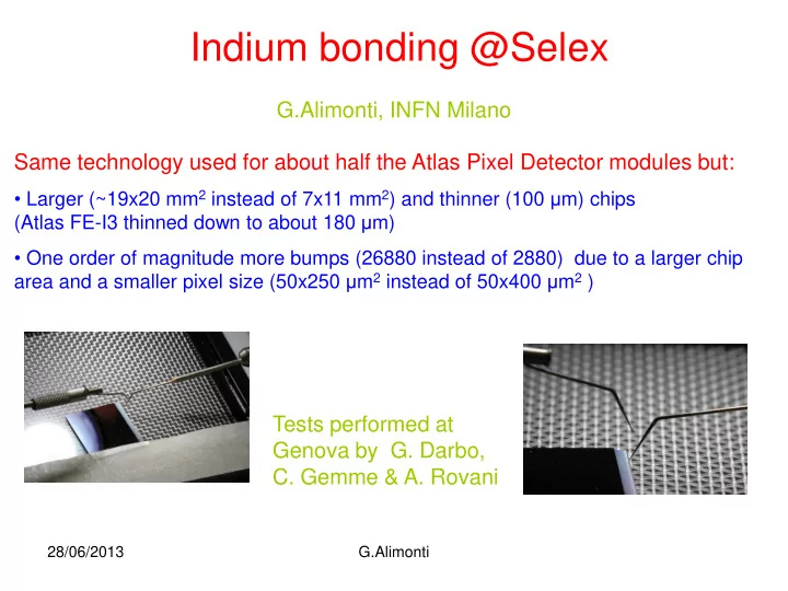
G.Alimonti, INFN Milano Same technology used for about half the Atlas Pixel Detector modules but:
- Larger (~19x20 mm2 instead of 7x11 mm2) and thinner (100 μm) chips
(Atlas FE-I3 thinned down to about 180 μm)
- One order of magnitude more bumps (26880 instead of 2880) due to a larger chip
area and a smaller pixel size (50x250 μm2 instead of 50x400 μm2 )
Tests performed at Genova by G. Darbo,
- C. Gemme & A. Rovani