hypothetical single cycle implementation of dlx

Hypothetical Single-cycle Implementation of DLX Assume Each - PowerPoint PPT Presentation

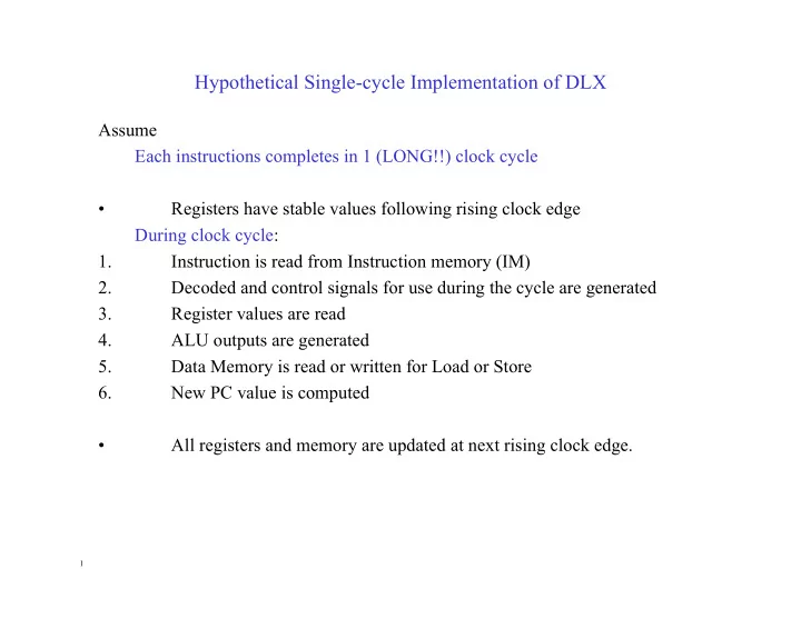
Hypothetical Single-cycle Implementation of DLX Assume Each instructions completes in 1 (LONG!!) clock cycle Registers have stable values following rising clock edge During clock cycle: 1. Instruction is read from Instruction memory (IM)


  1. Hypothetical Single-cycle Implementation of DLX Assume Each instructions completes in 1 (LONG!!) clock cycle • Registers have stable values following rising clock edge During clock cycle: 1. Instruction is read from Instruction memory (IM) 2. Decoded and control signals for use during the cycle are generated 3. Register values are read 4. ALU outputs are generated 5. Data Memory is read or written for Load or Store 6. New PC value is computed • All registers and memory are updated at next rising clock edge. 1
  2. Datapaths R-R, R-Imm, MUX lw, sw : MWRITE RDataSel DATA (rs) rs a p Cycle 3:Datapath for lw Register ALU rt (rt) File q ADDR MUX DM b + d c ALUSel ALUop rd MUX 4 WSel RWrite DATA EXT ALUop MREAD PC IM Rwrite ALUSel Decode RDataSel WSel MREAD MWRITE 2

  3. Execution of an RI instruction R-R, R-Imm, MUX lw, sw : MWRITE RDataSel DATA (rs) rs a p Register ALU rt (rt) File q ADDR MUX DM b + d c ALUSel ALUop rd MUX 4 WSel RWrite DATA EXT ALUop MREAD PC IM Rwrite ALUSel Decode RDataSel WSel MREAD MWRITE 3

  4. Single Cycle Design • Cycle time determined by longest instruction • No reuse of Functional Units (Separate IM and DM, ALU and Increment Unit) LW IM READ DECODE ADDRESS DATA MEMORY READ REG WRITE REG READ PC+4 ADD IM READ DECODE ADD REG WRITE IDLE REG READ PC+4 4

  5. Multi Cycle Implementation ALUWrite IR AWrite P C A p REG ALU MEM IRWrite ALU FILE PCWrite OUT B q MDR BWrite ALUop 4 MEMRead MDRWrite STATE MACHINE DECODER 1 5

  6. Multi-Cycle Design State Machine Model Instruction Fetch : IR = IM[PC]; S0 PC = PC+4 Instruction Decode: Generate Control Signals S1 A = REG[rs] B = REG[rt] ALUout = PC + Shift(SE(offset)) R-R : p= A q = B lw : p= A q = SE(d) sw : p= A q =SE(d) S2 S5 S8 beq : p = A; q = B; ALUout = p op q ALUout = p op q ALUout = p op q S10 Z = (p .eq. q); 10 R-R : lw : If (z == 1) PC = ALUOUT; S3 S6 sw : S9 REG[rd] = ALUout MDR = DM[ALUout] DM[ALUout] = B To S0 lw : S7 To S0 To S0 REG[rt] = MDR To S0 S6 S0 S1 S5 S7 S0 S1 S2 S3 S0 2 LD (5 cycles) ADD (4 cycles) 6

  7. Cycle 1 : Instruction Fetch Datapath IR P C A REG ALU MEM ALUout IRWrite PCWrite B MDR ALUop 4 MEMRead IR IR = MEM[PC] Assert PCWrite, IRWrite, MemRead CONTROL Set ALUop to ADD PC = PC+4 Set MUXes at ALU inputs and PC S0 S0 S1 7 FSM

  8. Cycle 2 :Datapath for LW rs PC AWRITE IR rt A ALU MEM ALUout REG B ALUWRITE MDR BWRITE ALUop Optimistic Reads of register file d Optimistic computing SE << of Branch target IR address CONTROL Set ALUop to ADD Set MUXes at ALU inputs Assert AWRITE, BWRITE, ALUWRITE S1 S5 FSM S0 S1 8

  9. Cycle 3 :Datapath for lw ALUWRITE PC IR A ALU MEM ALUout REG B MDR ALUop Set ALUop to ADD SE Set MUXes at ALU inputs Assert ALUWRITE IR CONTROL S5 S6 FSM 9 S0 S1 S5

  10. Datapath Control MUX PC IR A ALU MEM ALUout REG B MDR 4 MUX SE << 10

  11. Cycle 4: Datapath for lw PC IR A ALU MEM ALUout REG B MDR MEM READ SE << MDRWRITE Assert MEM READ IR Assert MDRWRITE CONTROL S6 S7 FSM 11 S0 S1 S5 S6

  12. Cycle 5: Datapath for lw PC IR A ALU MEM ALUout REG B rt MDR DATA RegWrite SE << Assert REGWRITE Set MUXEs for DEST REG and DATA IR CONTROL S7 S0 FSM S0 S1 S5 S6 S7 12

  13. Datapath Control IR rt A r MUX ALU ALUout d REG PC MEM B c MDR DATA SE << MUX 13

  14. Datapath Control IR A ALU ALUout REG MEM PC B MDR SE << MUX 14 PCSELECT

  15. Cycle 1 : Instruction Fetch Datapath IR P C A REG ALU MEM ALUout IRWrite PCWrite B MDR ALUop 4 MEMRead IR IR = MEM[PC] Assert PCWrite, IRWrite, MemRead CONTROL Set ALUop to ADD PC = PC+4 Set MUXes at ALU inputs and PC S0 S0 S1 15 FSM

  16. Cycle 2 :Datapath for BEQ AWRITE rs PC IR A rt ALU MEM ALUout REG B ALUWRITE MDR BWRITE ALUop Optimistic Reads of register file d Optimistic computing SE << of Branch target IR address CONTROL Set ALUop to ADD Set MUXes at ALU inputs Assert AWRITE, BWRITE, ALUWRITE S1 S10 FSM S0 S1 16

  17. Cycle 3 :Datapath for BEQ ALUWRITE PC IR A ALU MEM ALUout REG z PCWRITE B MDR ALUop Set ALUop to ADD SE Set MUXes at ALU inputs Assert PCWRITE if z equals 1 IR CONTROL S10 S0 FSM 17 S0 S1 S10

  18. Performance Model Processor Model m classes of instruction: I j , j = 1, …m Instructions of class I j require C j clock cycles to execute Clock Frequency = F (Hz = cycles/sec) Clock Period = 1/F (sec / cycle) Program Model Executes a total of N instructions: N j of class I j: N = ∑ j = 1, ..,m N j Program Execution Time (Clock Cycles) = ∑ j = 1, ..,m ( N j x C j ) Program Execution Time (sec) = T N = ( ∑ j = 1, ..,m N j x C j ) / F Average Cycles Per Instruction (CPI): Total number of cycles/ Instruction Count = ∑ j = 1, ..,m ( N j x C j ) / N Depends on both the processor and the mix of instructions in the program 18 LD (5 cycles) ADD (4 cycles)

  19. Processor performance measures Most useful metrics depends on the benchmark program being measured • Benchmark independent measures alone (e.g. clock speed) do not provide sufficient information • Multi-cycle design: Program with all BEQ instructions is 1.67 times faster than one with all LDs !! • Real processors: Relation between instruction mix and performance is complex • Instruction execution time may depend on context of instruction • Raises issues regarding choice of benchmark programs, degree and modes of optimization permitted, etc. • Imperative to understand the issues behind the performance numbers presented by different vendors • CPI (Cycles per Instruction): Average number of clock cycles to execute an instruction • • ∑ i = 1, ..,m ( N i x C i ) / N = ∑ i = 1, ..,m ( N i x C i ) / ∑ i = 1, ..,m N i • IPC (Instructions per Cycle): Average number of instructions executed per clock cycle • IPC = 1/ CPI • Sequential processors require several clocks for an instruction, so CPI > 1 and IPC < 1 • Simple Pipelining aims for an IPC of 1 • Superscalar,VLIW, SMT processor designs try to increase the IPC beyond 1 • MIPS (Millions of Instructions per second): • MIPS = 10 -6 x N/ T N = 10 -6 x F x ( ∑ i = 1, ..,m N i ) / ( ∑ i = 1, ..,m N i x C i ) • MIPS = 10 -6 x F (cycles/sec) x IPC (instructions/cycle) = 10 -6 x 1 / (Clock Period x CPI ) • Program Execution Time (microsec 1 0 -6 sec) • T N = N / MIPS = N x CPI x Clock Period (microseconds) = N x CPI / F(MHz) 19

Recommend


More recommend